
The FC201 is an efficient implementation of a general offset/gain/delay correction. In order for it to be used within a Diamond/FPGA system, the I/O interfaces are standardized to the model described by Diamond.
The FC201 firmware module is designed to correct a single digital data channel. Typically, each channel requires its own correction coefficients. Coefficients are loaded asynchronously and are applied prior to the next input cycle. Loading coefficients affects a reset of the module. The module will not accept ADC_IN samples until the first set of coefficients are loaded.
The module is useful for correcting ADC input as well as DAC output data streams.
FC201 – ADC/DAC Data Calibration
A calibration operation is required to normalize the output of each ADC/DAC (DAQ) within a multi-DAQ system. Variations in the manufacturing process of the DAQs and the surrounding circuitry can introduce voltage offsets and sampling gain variations on each channel. Further, external systems connected to the DAQs may not have complete control over all process parameters. Finally, when acquiring signals among multiple channels and multiple boards, (fixed) delays in the sampling clock may occur.
Each FC201 instance allows any digital data channel to be corrected at the rate that the data is produced. It acts as a digital filter to transform the data stream. The FC201 component can manipulate samples in magnitude and time. It is the responsibility of the end-user application to determine the appropriate coefficients provided to the FC201 component in order to operate properly.
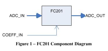
The firmware module operates in a flow-through mode; for every ADC_IN sample written, one ADC_OUT sample will be clocked out.