


PCIe104-RFSOC is based on the Xilinx XCZU27DR family in FFVG1517 package. This hardware is in PCIe104 form factor and adheres to its latest specification. It offers PCIe x1 Gen2.0 interface so 1 card could be connected to the ARM on the RFSOC device which acts as the host. The board also offers 1 PCIe x8 Gen 4.0, connected to the PL parts which can act both as host and end points. The additional interfaces offered by this card can be seen under the Features tab.
Depending on the choice of RFSOC on the board (25DR, 27DR and 28DR) it can offer addition logic, GPIO and GTYs through an on board LSHM connector.
One of the main features of the board is that all power to the RFSOC device are monitored for current and voltage and fed to the PL side.
The board also has superior clocking system to allow external clock and/or precise generation of clock speeds as required. The availability of TXCO clock with +-2.5ppm temperature tolerance provides additional stability.
The memory on this board is 8GB of DDR4 at 2400MHz and with ECC.
Power to the module is supplied through any standard PCIe104 power boards readily available on the market.
The ADC can be AC or DC coupled as a build option. The ADC input signals are differential and the DAC output are single ended.
There are connection for external clock and trigger and the clock is JESD204B compatible.
ADC and DAC can use builtin RFSoC PLL or use on board PLL LMX2954.
An LSHM connector provides access to 8GTY, x2 Ref clock, x1 PS GTR, x1 clock out, 24 PS side GPIOs, 24 differential GPIOs from the PL side connected to bank 66 and 7 to bank 65.
Features
- PCIe104 TYPE1 stack down Host with RF intrfaces
- populated with RFSoC XCZU25DR-2FFVG1517E as default but other options available
- for features of RFSOC use link above
- 8GB of DDR4 with ECC to PL and the same to PS
- JTAG
- 8 channels of ADC with differential input as AC or DC coupled as build option
- 8 channels of DAC as single ended output AC coupled
- external clock and trigger input with clock being JESD204B compatible
- Onboard TXCO oscillator with +-2.5ppm temperature tolerance
- 16GB of eMMC
- An LSHM connector provides access to 8GTY, x2 Ref clock, x1 PS GTR, x1 clock out, 24 PS side GPIOs, 24 differential GPIOs from the PL side connected to bank 66 and 7 to bank 65
- for the ARM processors within the device the following interfaces are available
-
- 1x USB 2.0/USB3.0
- Up to 8 GB of SDRAM via DDR4 ICs with ECC
- 1 x SATA
- 1 x RJ45 through headers
- USB UART
Applications
- Defense
- Aerospace
- Medical Imaging
- Control
- Instrumentation and testing
- Software Defined Radio
- Adaptable Radio platform
- Data capture and logging
|
 |
 |
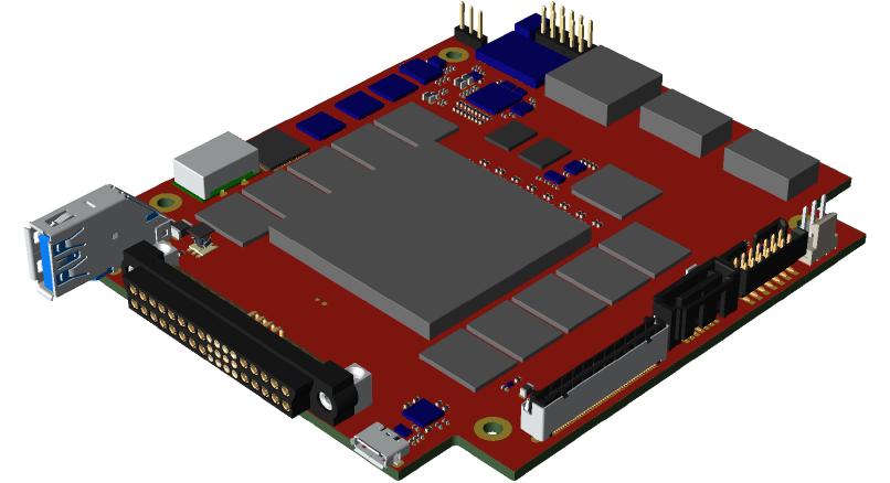 |
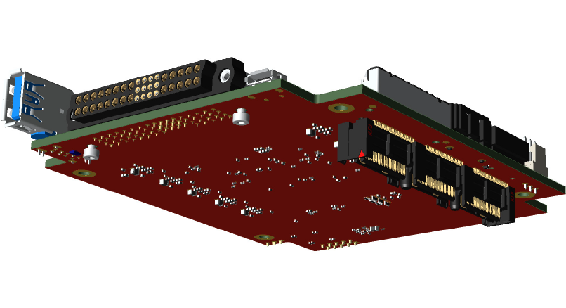
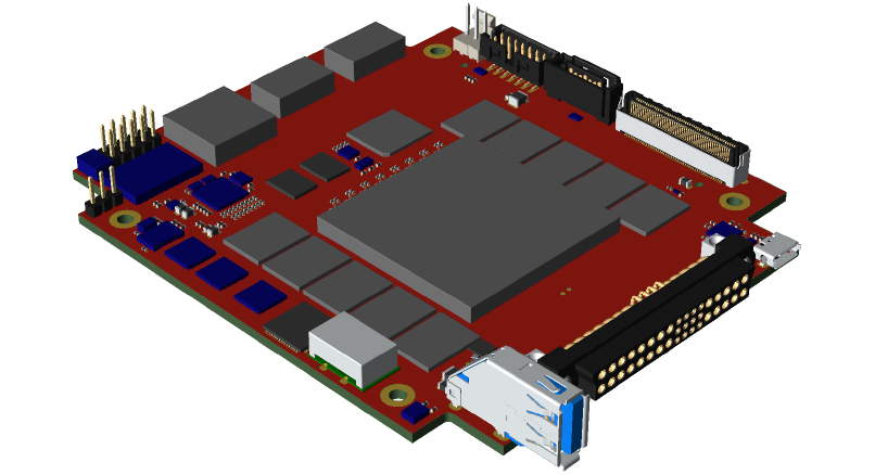
| Top view | Bottom view | Side view from left | side view from right |
3D model of PCIe104-RFSOC-with-heatsink
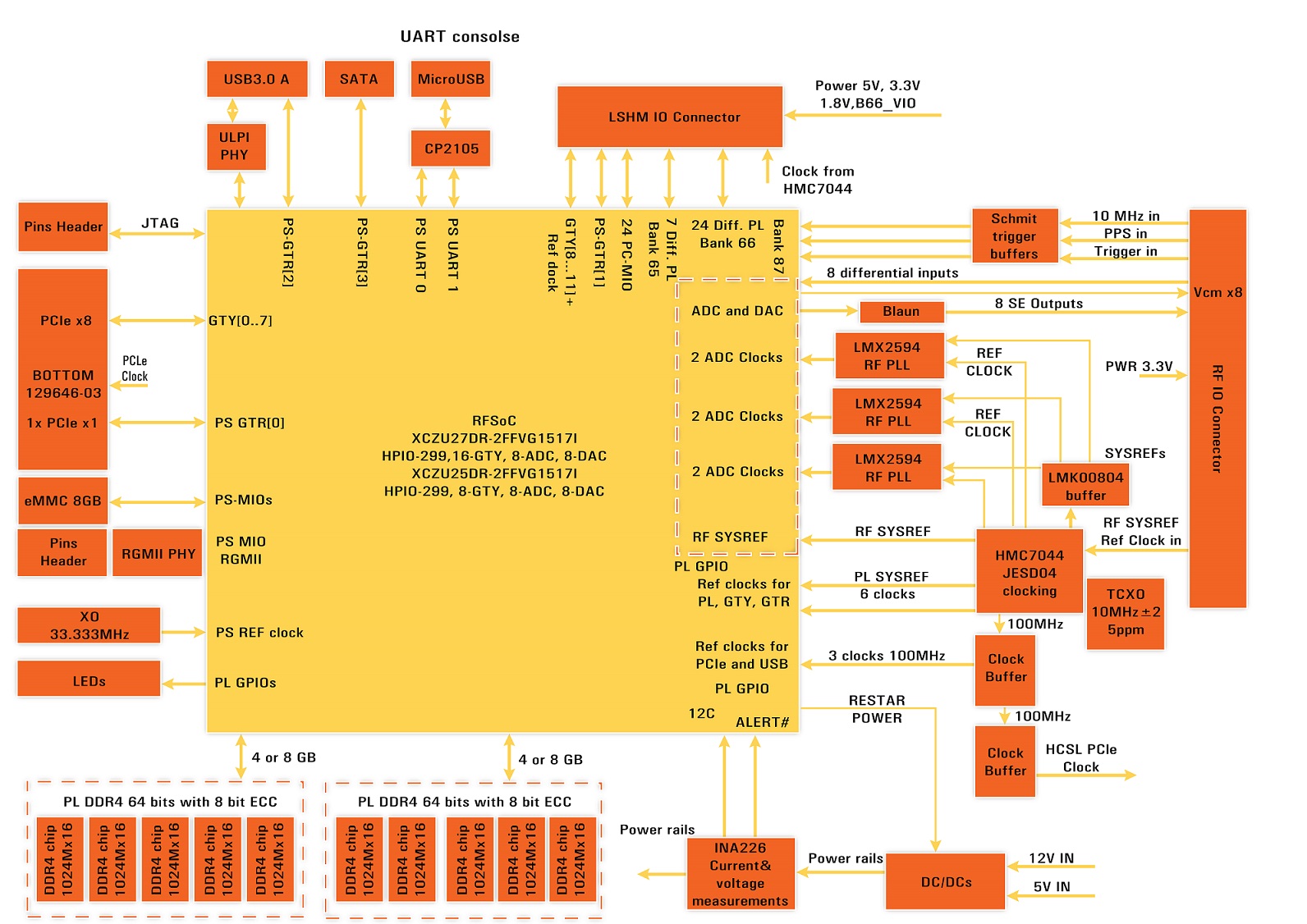
Block diagram
- PCIe104ZU-7CG-2-E – Dual A53 Core, Speed grade-2 & Extended Temp
- PCIe104Z-ZU7EG-2-E – Quad A53 Core, Speed grade-2 & Extended Temp
- PCIe104Z-ZU7EV-2-E – Quad A53 Core, Speed grade-2 & Extended Temp + H.265 CODEC
- PCIe104Z-ZU11EG-2-E – Quad A53 Core, Speed grade-2 & Extended Temp
All above can also be ordered in -I industrial grade which has a temp of -40 to 100deg C for the Zynq device.