
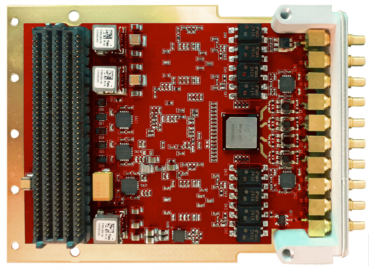

The FMC-ADC500CD is a cutting-edge HPC FMC module that offers 4 channels of high sampling rate and high-resolution ADC and DAC. Both the ADC and DAC interface to a carrier board using a JESD204B interface. The inputs of the ADC can be changed from AC coupled to DC coupled on the fly.
This board is designed for high-performance data acquisition and signal generation applications that require precise synchronization and low latency. It features the following components:
• HMC7044 from ADI: This is the main clock distribution IC that provides multiple clock outputs with SYSREF signals. It can clock JESD204B devices with subclass 1 synchronization.
• ADS54J60 from TI: These are dual-channel, 16-bit, 1-GSPS ADCs that support JESD204B interface. They can operate at various sample rates and enable decimation for lower bandwidth applications.
• DAC39J84 from TI: This is a quad-channel, 16-bit, 2.8-GSPS DAC that supports JESD204B interface. It can generate direct IF or RF signals with high dynamic range and low distortion.
• External trigger input: This allows adding timestamps to the sample stream from the ADCs for accurate timing measurements.
• Internal VCXO and TCXO clocks: These provide stable and low-jitter reference clocks for the board. The HMC7044 also generates SYSREF signals with known and adjustable delay for JESD204B synchronization.
With this board, you can achieve high-speed data conversion, signal generation, and synchronization for your applications. It is ideal for radar, wireless communication, test and measurement, and other demanding scenarios.
Features
• Two dual-channel ADS54J60 ADCs: These are 16-bit, 1-GSPS ADCs that support JESD204B interface. They can operate at various sample rates and enable decimation for lower bandwidth applications.
• One quad-channel DAC39J84 DAC: This is a 16-bit, 2.8-GSPS DAC that supports JESD204B interface. It can generate direct IF or RF signals with high dynamic range and low distortion.
• JESD204B interface via HPC connector: This provides 8 lanes of 12-Gbps data transfer per lane between the ADCs, DAC, and FPGA.
• HMC7044 clock generator: This is a high-performance, 3.2-GHz clock generator that provides multiple clock outputs with SYSREF signals. It can clock JESD204B devices with subclass 1 synchronization.
• External trigger input: This allows adding time stamps to the sample stream from the ADCs for accurate timing measurements. It has a logic LVTTL 3.3-V level.
• External clock input: This can be used as a reference clock or a main device clock input for the board. It can be connected to an external source or an internal VCXO or TCXO.
• 10 SSMC input connectors: These are used for the following purposes:
• 4 for single-ended input of ADC signal, with a frequency range of DC to 500 MHz.
• 4 for single-ended output of DAC signal, with a frequency range of 10MHz to 1.25 GHz (AC-coupled), option for DC-coupled 10MHz-200MHz (contact SDSP support for more information)
• 1 for trigger input, with a logic level.
• 1 for clock input, which can be used as a reference for the DAC and ADC via PLL.
• JESD204B subclass 1 capability: This means that the board can achieve precise synchronization and deterministic latency between multiple JESD204B devices using REF CLK and SYSREF signals.
• 100-MHz ±12-ppm onboard VCXO: This is a voltage-controlled crystal oscillator that provides a stable and low-jitter reference clock for the board.
• 10-MHz ±1.5-ppm onboard TCXO: This is a temperature-compensated crystal oscillator that provides another option for a reference clock for the board.
• RF inputs: These are single-ended, 50-Ohm, 1.9-Vpk-pk inputs that can be DC or AC coupled (selected by firmware).
• RF outputs: These are single-ended, 50-Ohm, 1-Vp-p outputs that can generate IF or RF signals.
• Vadj supported voltages: These are 1.8 V, 2.5 V, and 3.3 V, which can be used to power different components on the board.
• Power consumption: This is TBD (to be determined).
Applications
- Defense
- Intelligence
- Wireless communications
- Broadcast equipment
- Medical equipment
- Test and measurement equipment
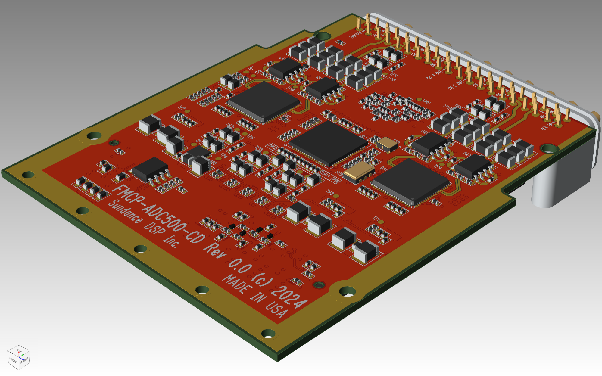 |
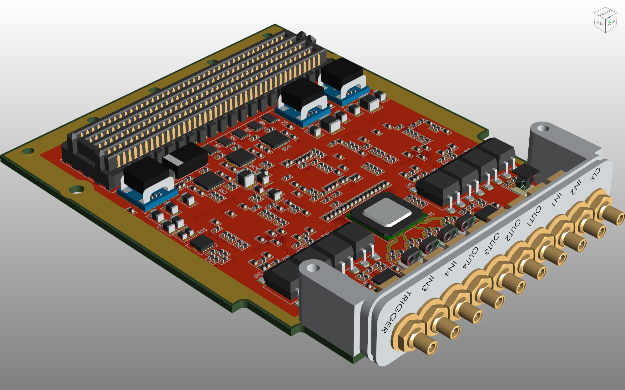 |
| FMC-ADC500CD Solder Side | FMC-ADC500CD Component Side |
Block Diagram
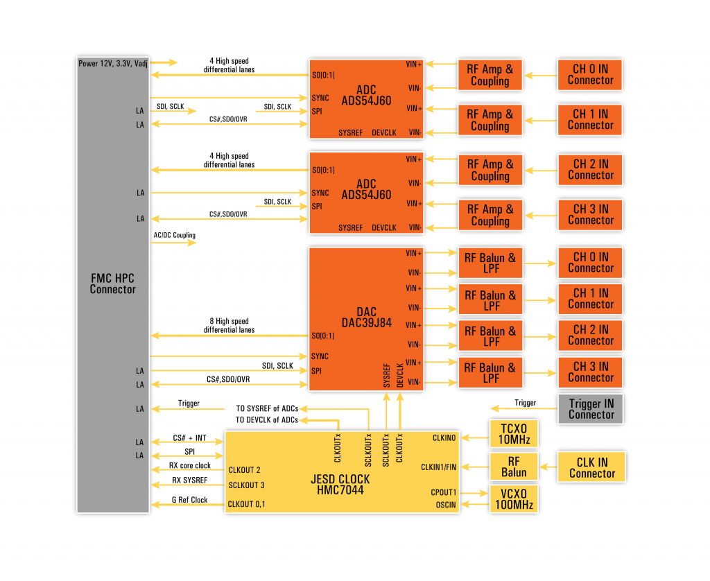
Polar VPX block diagram
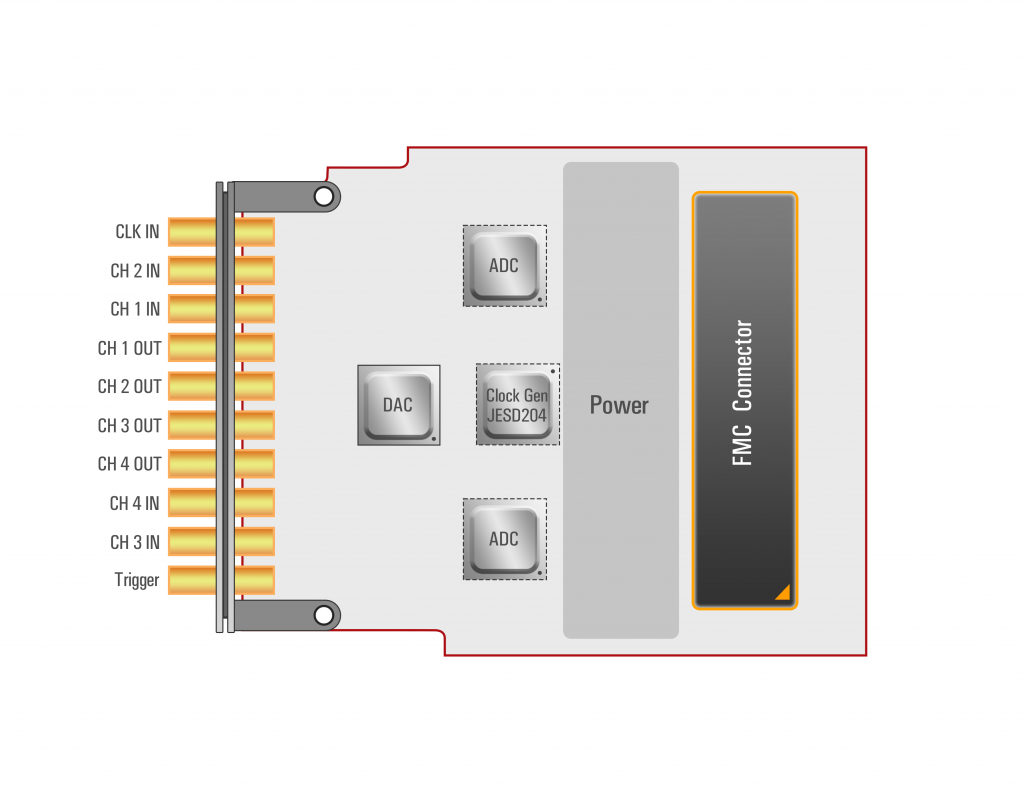
Placement diagram
A full BSP including Buildroot Linux for a Zynq US+ MPSOC device will be included which works with SDSP’s SE120 11eg card will be provided along with ADI drivers.
FMC-ADC500CD
Contact SundanceDSP support if a different temperature grade or if a custom configuration is required.