

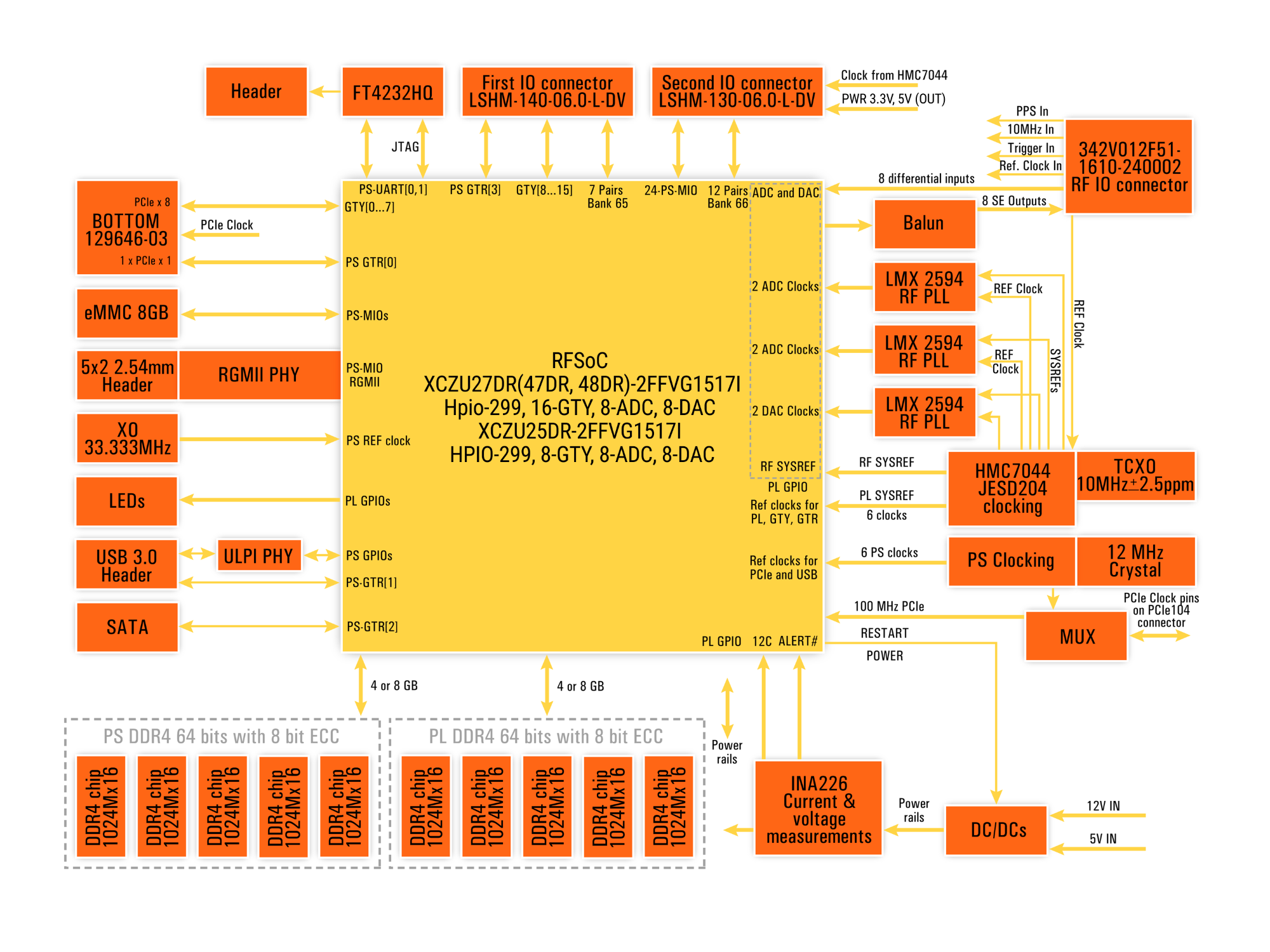
PCIe104-RFSOC is based on the AMD XCZU47DR-2FFVG1517E RFSOC device (optional 27DR and 48DR can be used with -E or -I temperature grades). The RFSOC development board is in PCIe104 form factor and electrically adheres to its latest specification. This is a TYPE 1 Host board with only Stack Down connections supported. One lane of PCIe from the PS side is routed to Bank 1 of the PCIe104 connector and x8 Gen 3.0 PCIe from PL side is available from the other banks.
8GB of DDR4 memory with ECC is attached to the PL and 8GB with ECC is connected to the PS side. Micron MT40A1G16RC-062E IT:B is utilized in this design. 32GB of eMMC is placed on the board and can be used for storing the firmware and/or Linux image for the PS side.
The module provides up to 8ADC and DAC channels via the Nicomatic RF connector part number 342V012F51-1610-240002. And Sundance supplies the mating connector and cable part number C19993-0203. Please see images of cable assembly in “additional Images” tab.
ADC channels support 12bit 4.096GSPS with / DDC; and DAC channels can achieve 14bit 6.554GSPS with / DUC (higher rates available if using the Gen 3 RFSoC devices).
The 8 channel DAC outputs are configured as single ended and go through Baluns but the 8 channel ADC Input are configured as differential inputs for maximum accuracy. The clocking IC for the RF channels is LMX2594.
A PPS GPS signal input signal is possible to input via the RF IO connector with an external 10MHz clock. The Ref clock IN and Trigger In are also provided via the RF IO connector (it is optional to provide these inputs, clocking for all interfaces is present on the board by default).
Two IO connectors in the form of Samtec LSHM connectors offer additional IOs and transceivers from the PS and PL sides for user applications.
This module is Made in USA.
Features
- Main device is the Xilinx RFSoC XCZU27DR-2FFVG1517E, compatible with ZU47DR, and ZU48DR. Other temperature grade like -I are also available (also RFSOC GEN1, 2, and 3 are compatible);
- PCIe104 stack-down connector, PCIe104 TYPE 1 HOST board;
- PCIe x8 GEN 3 Root Complex (RC) from PL part;
- One PCIe x1 RC interface from PS, connected to Bank 1 of PCIe104 connector;
- 5×2 2.54mm header connector for 100/1000Base-T interface;
- One SATA connector with Gen 3.0 interface;
- 5×2 2.54mm header with USB 3.0, HOST, interface;
- 5 pins 2.54mm header with USB- JTAG/UART Bridge IC FT4232HQ;
- Five Single Die 1024×16 DDR4 chips for PL – 72 bit bus width(total 8GBytes), default part number is MT40A1G16RC-062E IT:B
- Five Single Die 1024×16 DDR4 chips for PL – 72 bit bus width(total 8GBytes), default part number is MT40A1G16RC-062E IT:B
- 16 GByte of eMMC as boot and OS storage, other eMMC capacity is available as build option;
- RF IO connector is 342V012F51-1610-240002 from Nicomatic;
- Two IO connectors are LSHM-130-06.0-L-DV-A-S-K-TR and LSHM-140-06.0-L-DV-A-S-K-TR;
- Eight ADC channels are differentially routed to the RF IO connector; as build option, they can be AC or DC coupled, so on an RF IO board, the user can create any input network;
- Eight DAC channels, routed to the RF IO connector; the output is 50 Ohm, AC coupled, and single ended;
- Built in RFSoC ADC – 12bit 4.096GSPS with / DDC (more if using RFSOC Gen 2 or Gen 3)
- Built in RFSoC DAC – 14bit 6.554GSPS with / DUC (more if using RFSOC Gen 2 or Gen 3)
- PPS GPS signal input, from the RF IO connector;
- External 10MHz clock input from GPS, from the RF IO connector;
- User reference clock input from the RF IO connector;
- Trigger In from the RF IO connector;
- INA226 IC for current and voltage monitoring, for FPGA power supply, the I2C interface is connected to the PL side of the device;
- Eight GTY transceivers (not available on XZCU25DR) with three reference clock inputs, routed to the first LSHM IO connector;
- One PS-GTR transceiver routed to the first IO connector.
- 7 Differential Pairs from HP Bank 66 routed to the first IO connector.
- I2C from the PS with 1.8V level and one clock output routed to the second IO connector.
- 22 PS-MIOs with 3.3V level, from PS part routed to the second LSHM IO connector.
- 12 Differential Pairs from HP bank 65 are routed to the second IO connector, levels 1.8V by default, it can be changed by an ordering option to be 1.2V if required;
- Power can be delivered on the 5V and 3.3V rail at 1Amp of current both supplies are available on second IO connector for external usage;
- The main clocking IC is HMC7044, and it can be synchronized with a user reference clock;
- ICs for clocking DAC and ADC are LMX2594;
- LEDs for power good signals;
- Two Green user LEDs on the board;
- Operating temperature range, -40°C to +85°C;
- Maximum board power consumption is estimated to be 80 Watts;
Applications
- Defense
- Medical Imaging
- Machine Vision
- Stereo vision
- Artificial Reality /Augmented Reality
- Control
- Instrumentation and testing
- Software Defined Radio
- Data capture and logging
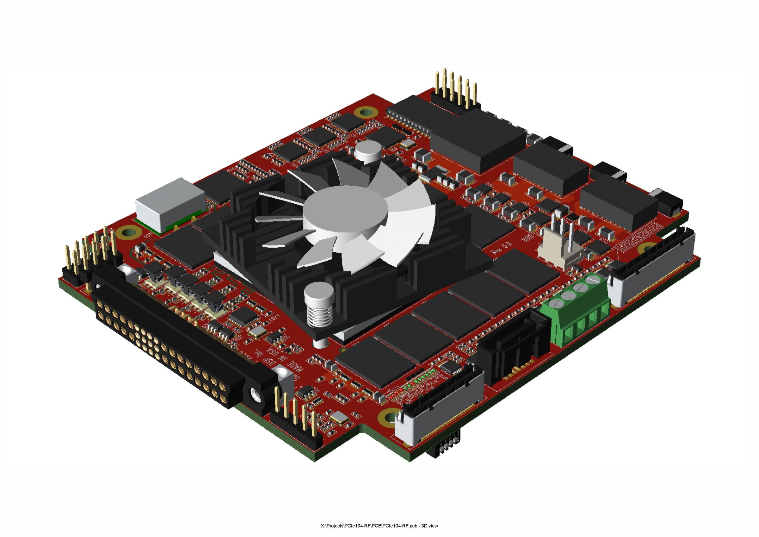
3D model of PCIe104-RFSOC-with-heatsink
Block diagram of PCIe104 RFSOC
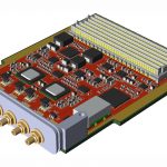
Component side
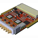
PCIe104-RFSOC
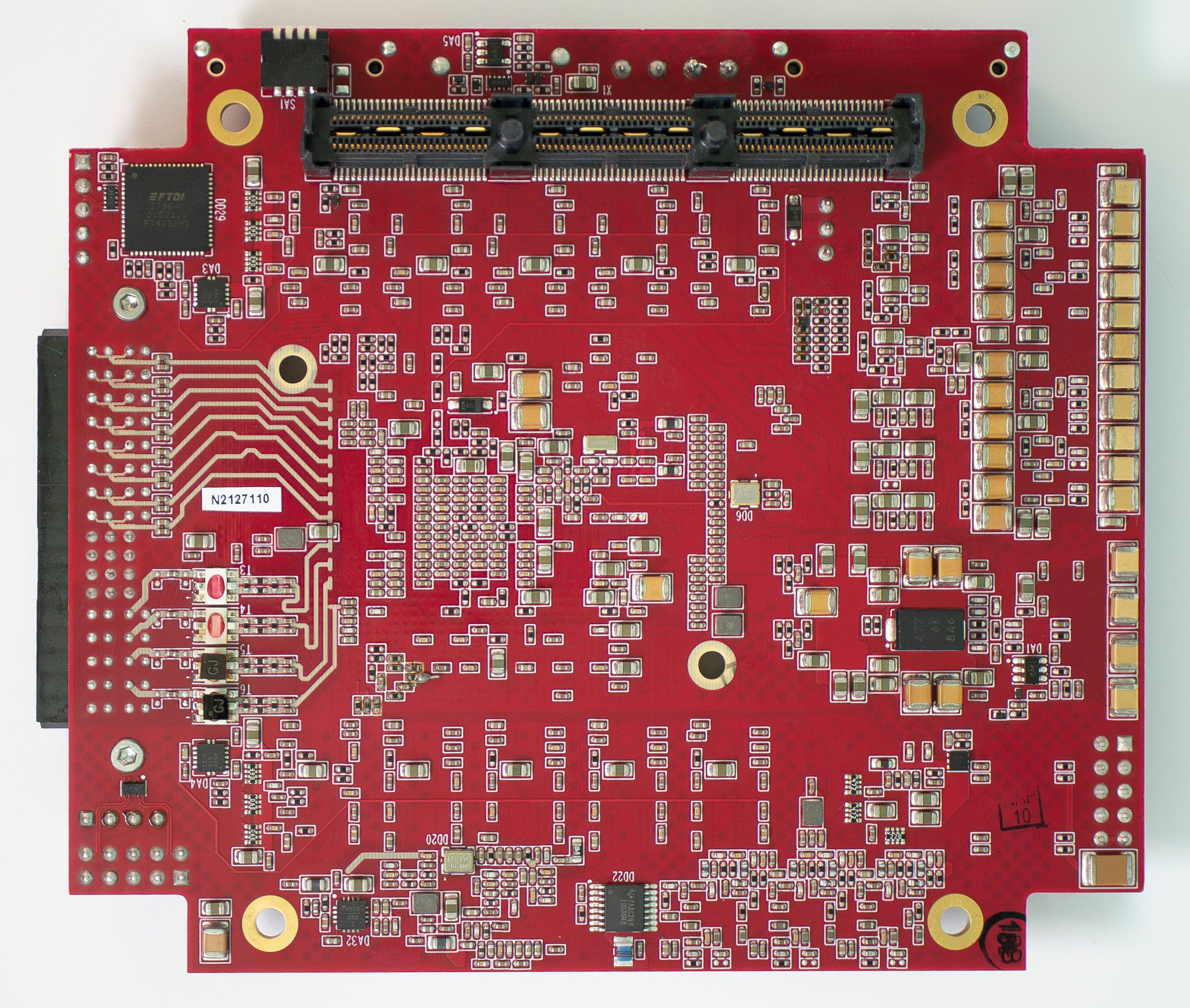
Solder side
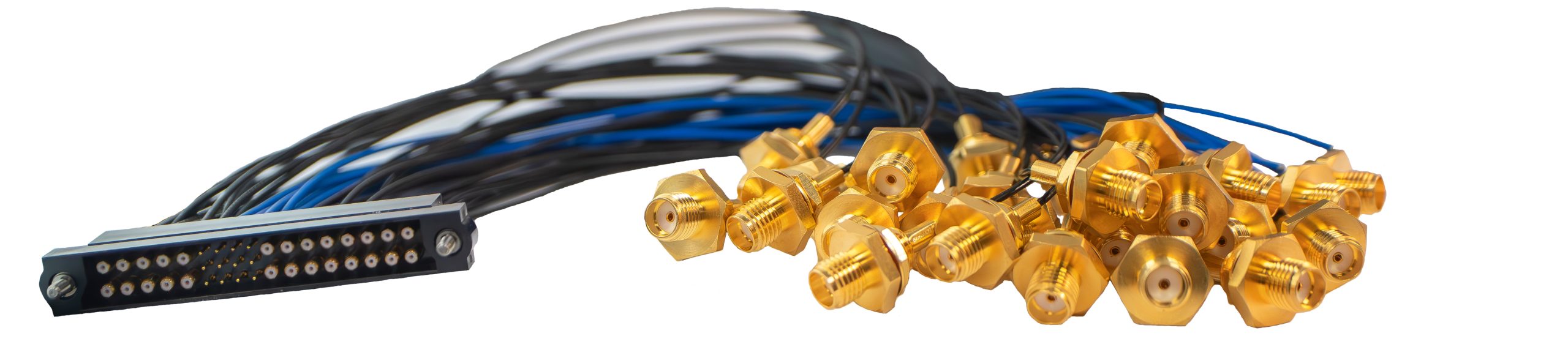
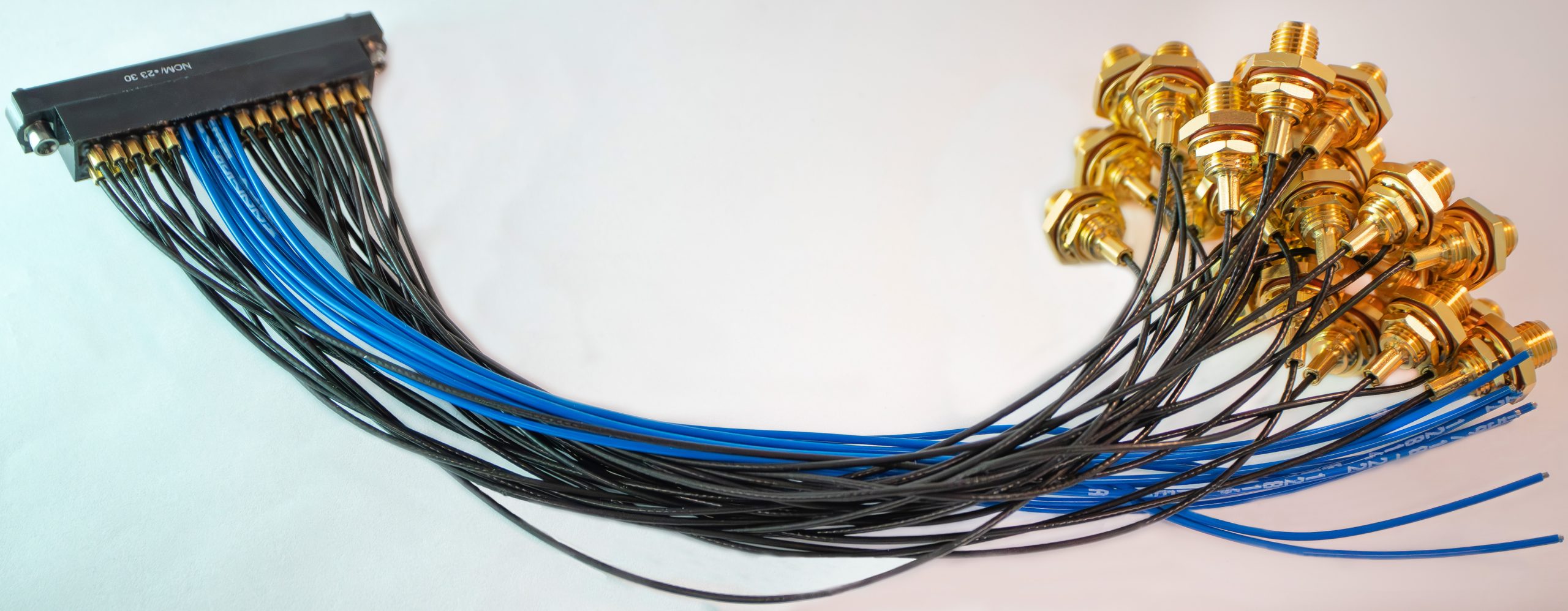
RF Cable assembly
- PCIe104-RFSOC-xxDR-T-S
where as xx can be 25, 27, 28, 47 or 48, T is temperature grade and it can be -E or -I and S is the Speed grade and can be 1 or 2