
The FG650 pairs the FMC-CL mezzanine module with the SE120 carrier board to form a complete, FPGA-based solution for capturing and processing four Camera Link streams in real time. The FMC-CL handles the physical I/O for up to four connectors, while the SE120 hosts the main IP core that decodes, aligns, and reformats the raw Camera Link data into image frames ready for on-chip processing.
Key Components
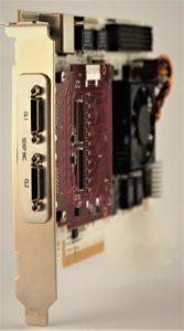
FMC-CL Module
- Dual full/extended Camera Link interfaces, each supporting Base, Medium, Full, Extended Full, and dual-Base modes (up to four connectors total)
- LVDS I/O routed through FMC HPC (first interface) and FMC headers (second interface)
- Power-over-Camera-Link (PoCL) support on both connectors (12 V up to 333 mA per connector)
- ESD protection on all external pins
- Optional SATA lanes for direct disk connections
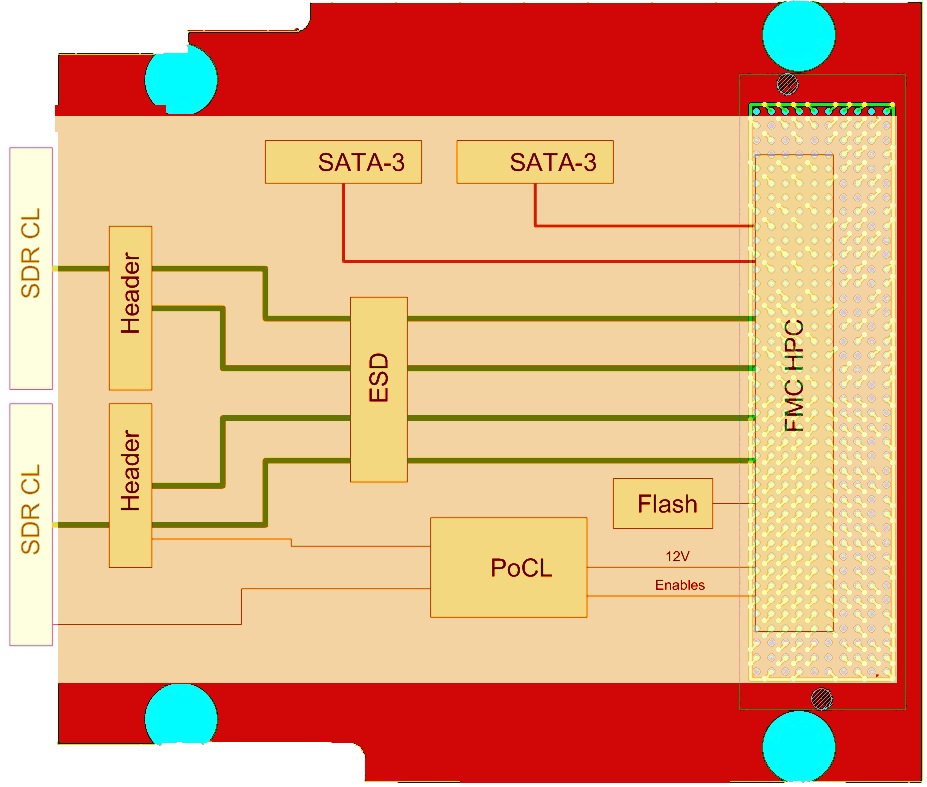
Figure 1: FMC-CL Block Diagram
SE120 Carrier Board
- AMD Zynq UltraScale+ MPSoC (XCZU11EG-2FFVC1156 by default) with PCIe Gen3 x8 endpoint
- High-pin-count FMC site for up to 10 GTH transceivers and 80 differential I/Os
- 4 GB DDR4 attached to PL (32-bit wide) and up to 8 GB DDR4 on PS side (64-bit ECC)
- Multiple high-speed interfaces: GigE, SFP+, USB 3.0, SATA 3.0, DisplayPort 1.2, CAN, UART, I²C
- Programmable clock generator (Si5341A) for reference clocks to PS, GTR lanes, and FMC
- Samtec high-speed connector for user-defined I/O and power rails
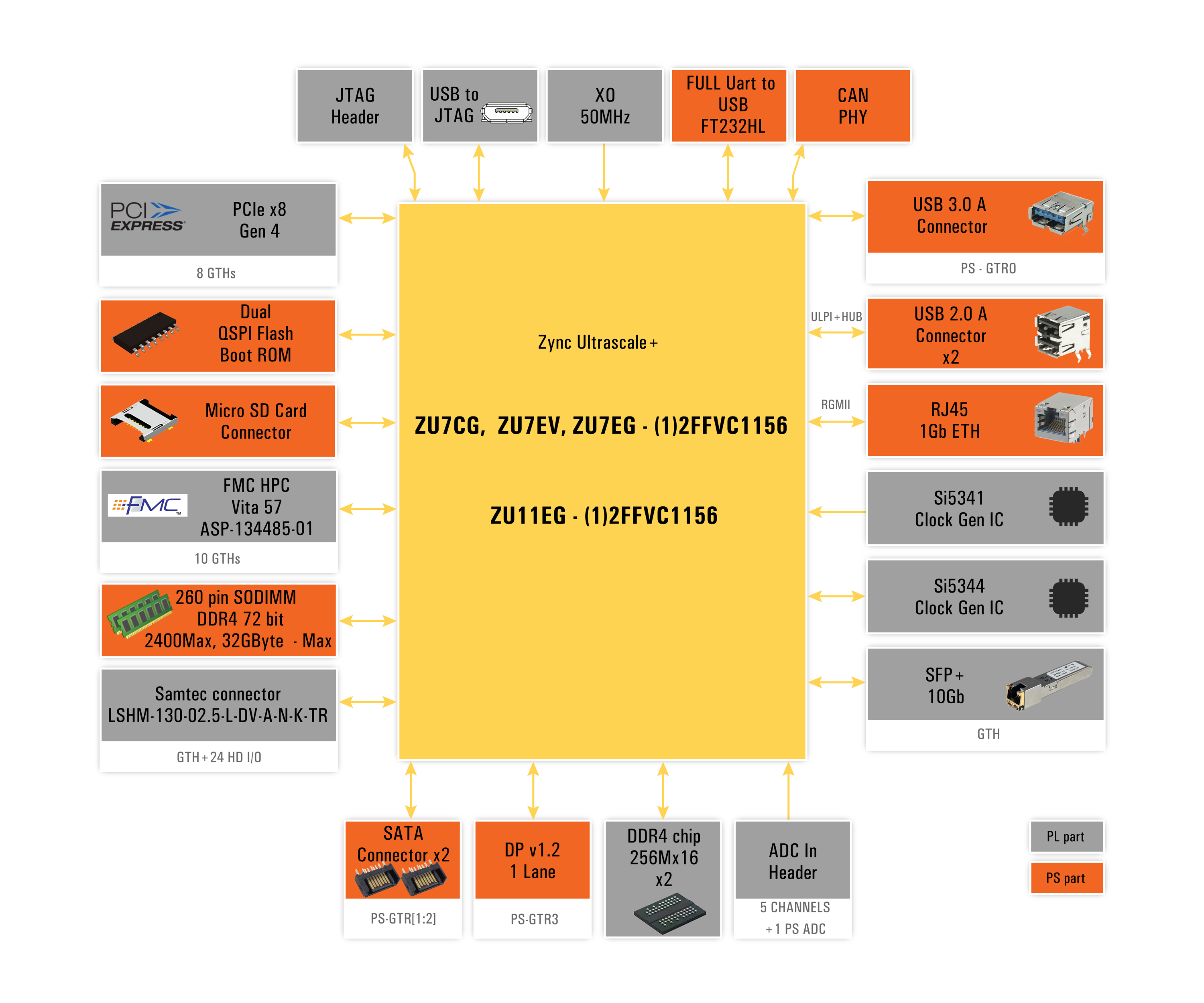
Figure 2: SE120 Block Diagram
Internal Data Path
Overview
- Camera streams arrive over up to four Camera Link cables.
- FMC-CL de-serializes LVDS lanes and presents them to the FPGA fabric.
- The CL-IP core on SE120 decodes each link, removes blanking, and extracts pixel data.
- Gearbox IP cores strip unused bits and align data widths.
- AXI-DMA moves reconstructed frames into DDR RAM.
- Host PC or on-chip logic reads frames via PCIe or PL fabric.
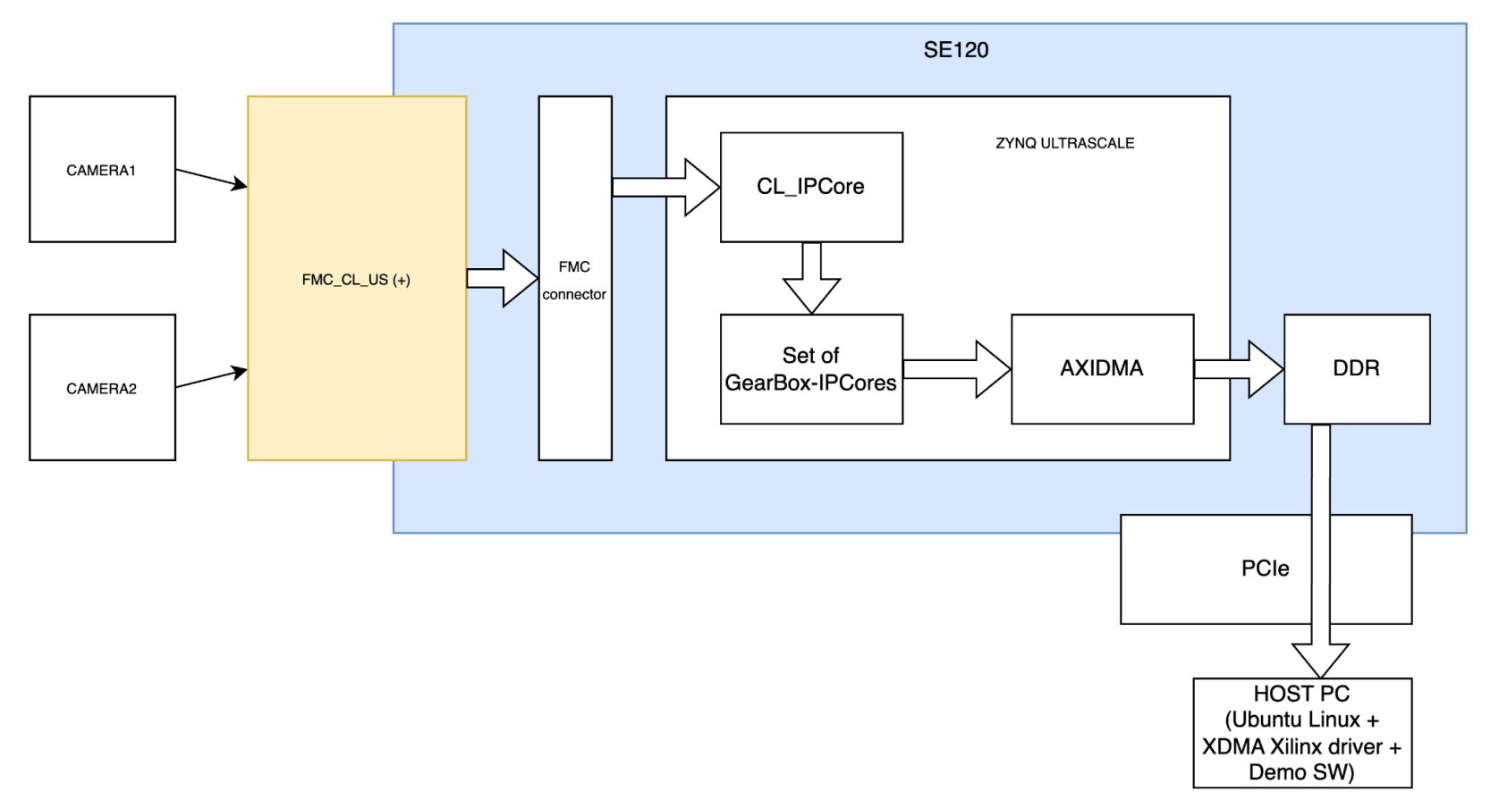
Figure 3: FG650 Internal Data Path
Camera Link Interface (AXI-CL-R Core)
- AXI-Lite slave for register access and core setup
- AXI-Stream master for pixel data output
- Key registers (32 bits each):
-
- CAMERA_RST_REG: Reset deserializer
- CAMERA_MODE_REG: Set Camera Link mode and bit depth
- CAMERA_CTRL_REG: Control camera channel timing
- CAMERA_PoCL_REG: Enable PoCL on each connector
- CAMERA_PACSIZE_REG: Define packet size (TLAST generation)
- CAMERA_TRIG_REG: Start/stop capture per camera
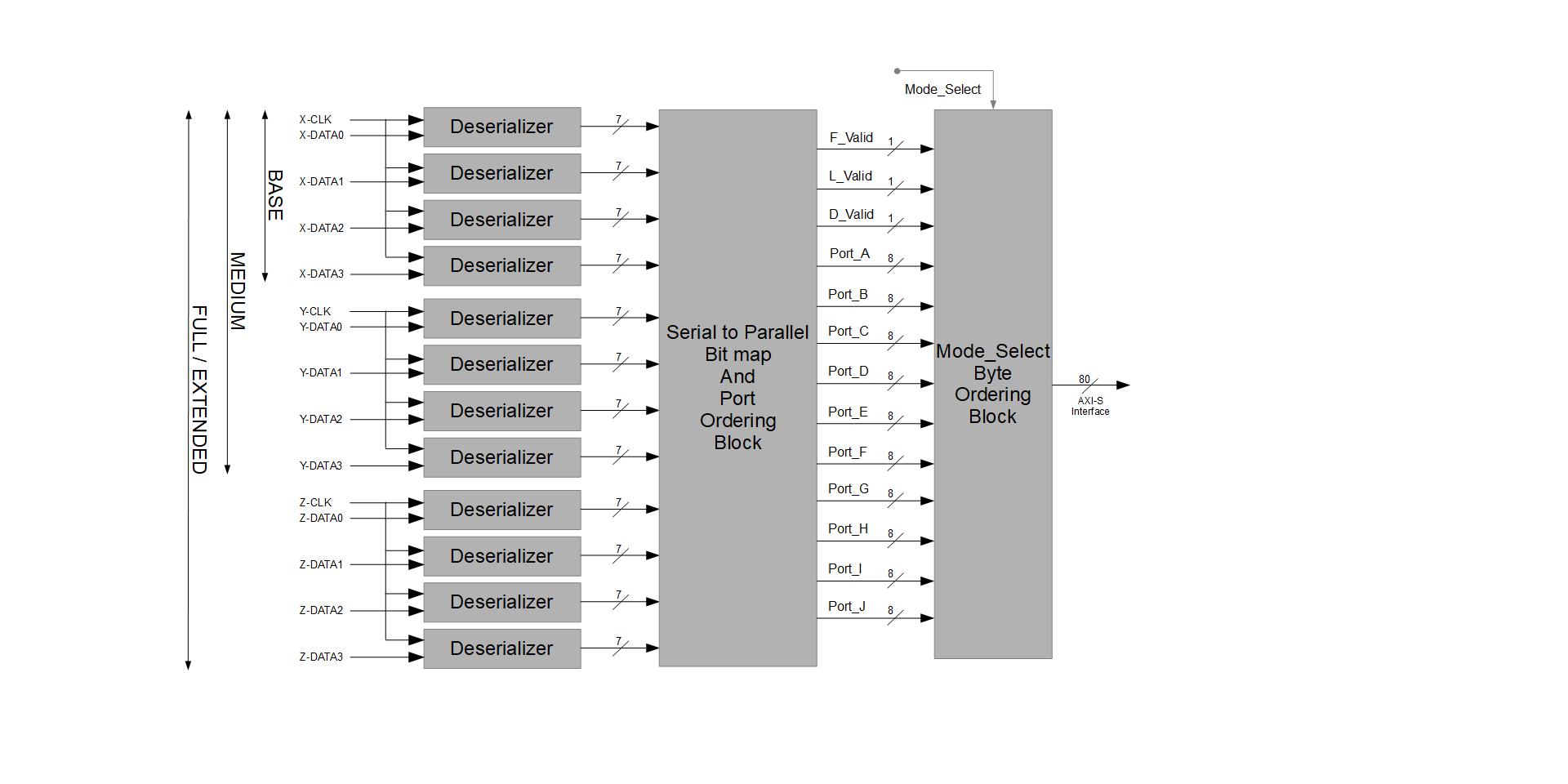
Figure 4: FG650 IP Core Block Diagram
Gearbox and DDR Storage
- Gearbox IP cores realign lanes (e.g., from 80 bits to 64 bits) and drop filler bits
- After the gearbox stage, the data is fully reconstructed into image-frame format, pixels are aligned into rows and columns, with frame boundaries marked, making it immediately suitable for further FPGA-based processing (e.g., AI inference, filtering)
- AXI-DMA engine writes streams to PL-DDR in scatter-gather lists
- PCIe XDMA transfers frame buffers to host memory
Frame Reconstruction in FPGA
Raw Camera Link data is a continuous LVDS stream without inherent frame markers. The IP core rebuilds frames by:
- Detecting timing signals (LVAL/HVAL) that mark active pixel windows
- Counting rows and columns based on camera resolution settings
- Asserting TLAST and TUSER on AXI-Stream for frame start/end
- Delivering an image-buffer layout in DDR: line-major order, pixel-packed
This output mimics a classic frame buffer, so downstream FPGA logic or embedded compute engines can consume it as standard image arrays.
Configuration and Setup
- Power up SE120 with FMC-CL attached.
- Load the FPGA bitstream (includes AXI-CL-R, Gearbox, XDMA).
- Via AXI-Lite registers:
- Reset CL IP: write
0x1to offset0x00 - Set mode (Base/Medium/Full/Extended) and bit depth at offset
0x04 - Enable PoCL if needed in the offset
0x0C - Select the camera connector in offset
0x10 - Define the packet size at the offset
0x14 - Trigger capture at offset
0x18
- Reset CL IP: write
- Prepare DMA SG list (use host API or demo application).
- Start the AXI-DMA engine and read out frames over PCIe.
On-Chip Image Processing
Once frames reside in PL-DDR as standard buffers, you can:
- Run convolution kernels or edge filters
- Feed data to AI inference IP blocks (e.g., object detection, classification)
- Stream processed frames back to the host or output via video I/O ports
The FG650’s FPGA-centric pipeline eliminates CPU parsing overhead, delivering sustained, low-latency, multi-camera throughput at full Camera Link rates.
Source Code and Licensing
The complete FPGA firmware source code is available for purchase by interested parties. This includes the full Vivado project, HDL files for the AXI-CL-R core, gearbox logic, and DMA engine integration. By acquiring the source, you gain full visibility into the design and can adapt or extend it to your specific application.
The Camera Link IP core itself is offered on a royalty-free basis. Once you purchase the firmware source, you may integrate the IP core into your own systems without any ongoing license fees or per-unit royalties. This approach lets you:
- Modify or enhance the core to match your performance or feature needs
- Distribute your custom bitstreams without extra payments
- Rely on a single, predictable upfront cost for long-term deployments