

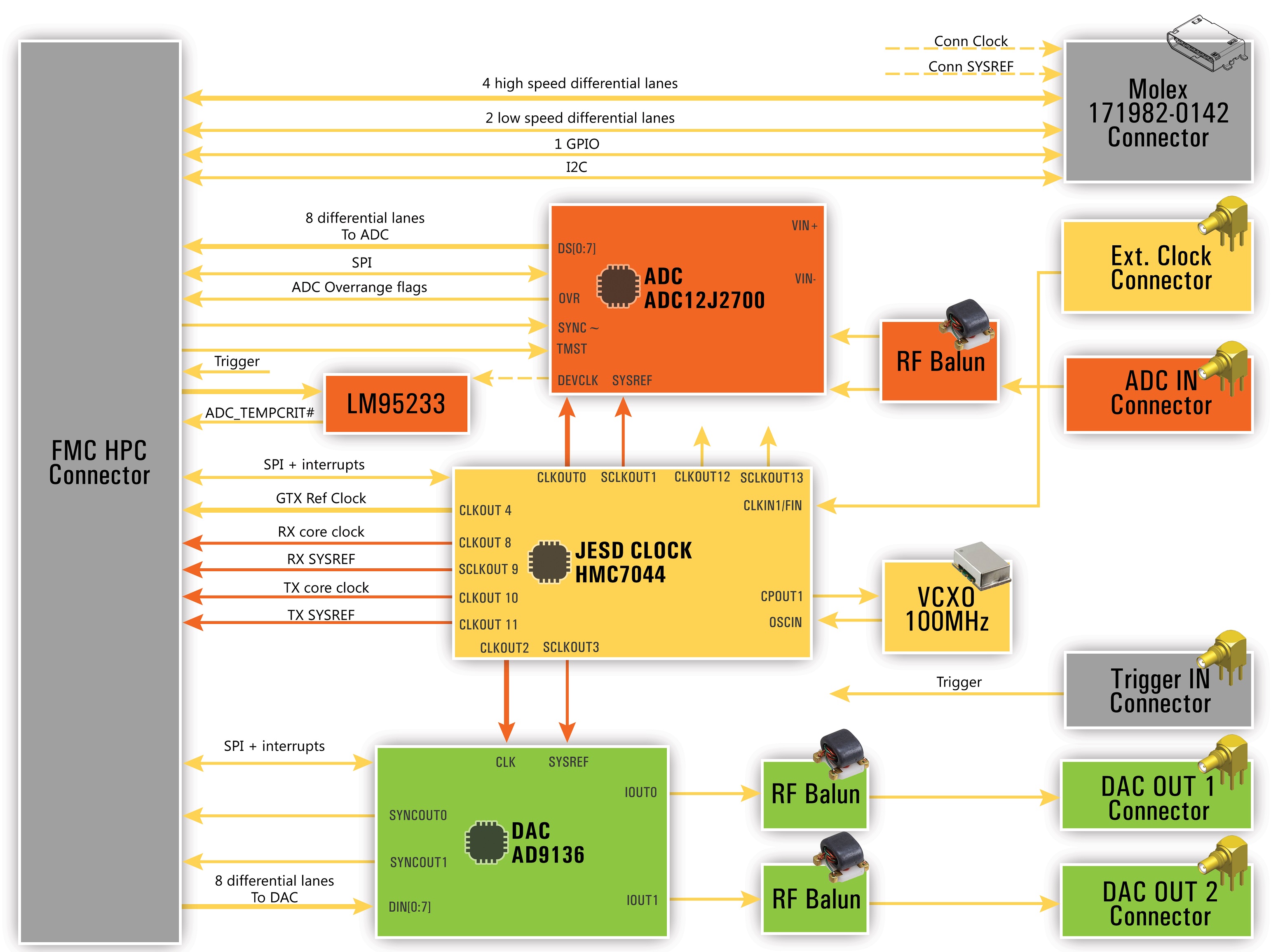
FMC-DAQ2P5 allows for ADC decimation and DAC interpolation. External trigger input allows the addition of timestamps to the sample stream from ADC. CLK-IN can be a Sample clock input up to 4GHz, or a reference clock input up to 1GHz. The module provides simultaneous working of ADC and DAC on a sample rate of 2.1GSPS, using an internal VCXO clock.
FMC-DAQ2P5 provides 4 x high-speed transceiver lanes routed from the FPGA carrier card to the bezel. 4 differential low-speed lanes and 10 single-ended IO are also routed to the Molex connector available at the bezel which, can be used for any control or data exchange with the FPGA.
ADC Parameters
- 12-Bit Resolution, single-Chanel, 2.7-GSPS ADC
- Noise Floor: –146 dBFS/Hz
- INL: ±2 LSB (Ta = 25)
- DNL: ±0.25 LSB (Ta = 25)
- Spectral Performance (fIN = 600 MHz at –1 dBFS):
- SNR: 54.8 dBFS
- NSD: –146 dBFS/Hz
- SFDR: 71.6 dBFS
- ENOB: 8.8 Bits
- Spectral Performance (fIN = 1500 MHz at –1 dBFS):
- SNR: 52.5 dBFS
- SFDR: 65.2 dBFS
- THD: -68 dBFS
- Input Full-Scale differential: 0.95 VPP
- Full power Bandwidth (-3 dB – calibration = FG): 3200 MHz
- Integrated Wideband DDC Block
- Input type: AC – coupled, single ended.
- Input frequency range: 30 – 1800 MHz
- Maximum input voltage – 2 Vpp single ended
- Power Dissipation: 2.21 W max at 2.7 GSPS
DAC part parameters
- Resolution: 16-Bit
- Maximum Sample Rate: 2.8GSPS
- Maximum Input Data Rate: 2.12GSPS
- 8 JESD204B Serial Input Lanes
- 10.6 Gbps Maximum Bit Rate per Lane
- Subclass 1 -DAC Synchronization
- On-Chip Very Low Jitter PLL
- Selectable 1x –8x Interpolation
- Sinx/x Correction Filters
- 3/4-Wire Serial Control Bus (SPI)
- Outputs: AC coupled, transformer-isolated
- Output voltage range: 2Vpp max
- Output frequency range: 20 – 1060 MHz
- Integrated Temperature Sensor
- Power Dissipation: 1.74W at 1.6GSPS
Clock and trigger in parameters
- External clock in the frequency range, in reference clock mode – 10 – 800MHz
- External clock in the frequency range, in device clock mode – 400 – 4000MHz
- Input: AC coupled, 50 Ohm, single-ended.
- Input power range: -6 to 6 dBm.
- Trigger input – logic level, ESD protected, LVTTL 3.3V
Features
- 1 x ADC 12 bit @ 2.7 GSPS
- 2 x DAC 16 bit @ 2.8 GSPS
- High Pin Count ( HPC ) FMC module
- PXIe, PCIe, Stand-Alone … platforms
- Trigger Input
- External Clock up to 4 GHz
- 100 MHz onboard VCXO
- 4 x high-speed and 4 x low-speed differential lanes
- 10 x single-ended IOs
- Optional dual SATA for direct disk interface
- Commercial and Industrial grades
Applications
- Radar / Sonar
- Wireless communication transceivers / base stations
- Defense / Aerospace / Satellite communications
- Medical
- Automotive
- Direct RF Down Conversion
- Test and measurement
- Beamforming / Directional vector
- Software-defined radio (SDR)
| FMC_DAQ2p5 | This is the default model with 1 ADC channel and 2 DAC channels. |
| FMC_DAQ2p5_ADC | The module will come with ADC. DAC will not be populated. |
| FMC_DAQ2p5_DAC | The module will come with DAC. ADC will not be populated. |
| PXIe700_FMC_DAQ2p5 | A PXIe700 with attached FMC-DAQ2p5 (1 channel of ADC and 2 channels of DAC) and complete IP core project for using the ADC and DAC channels through Xilinx JESD core (user needs to purchase their copy of Xilinx JESD IP core). |