
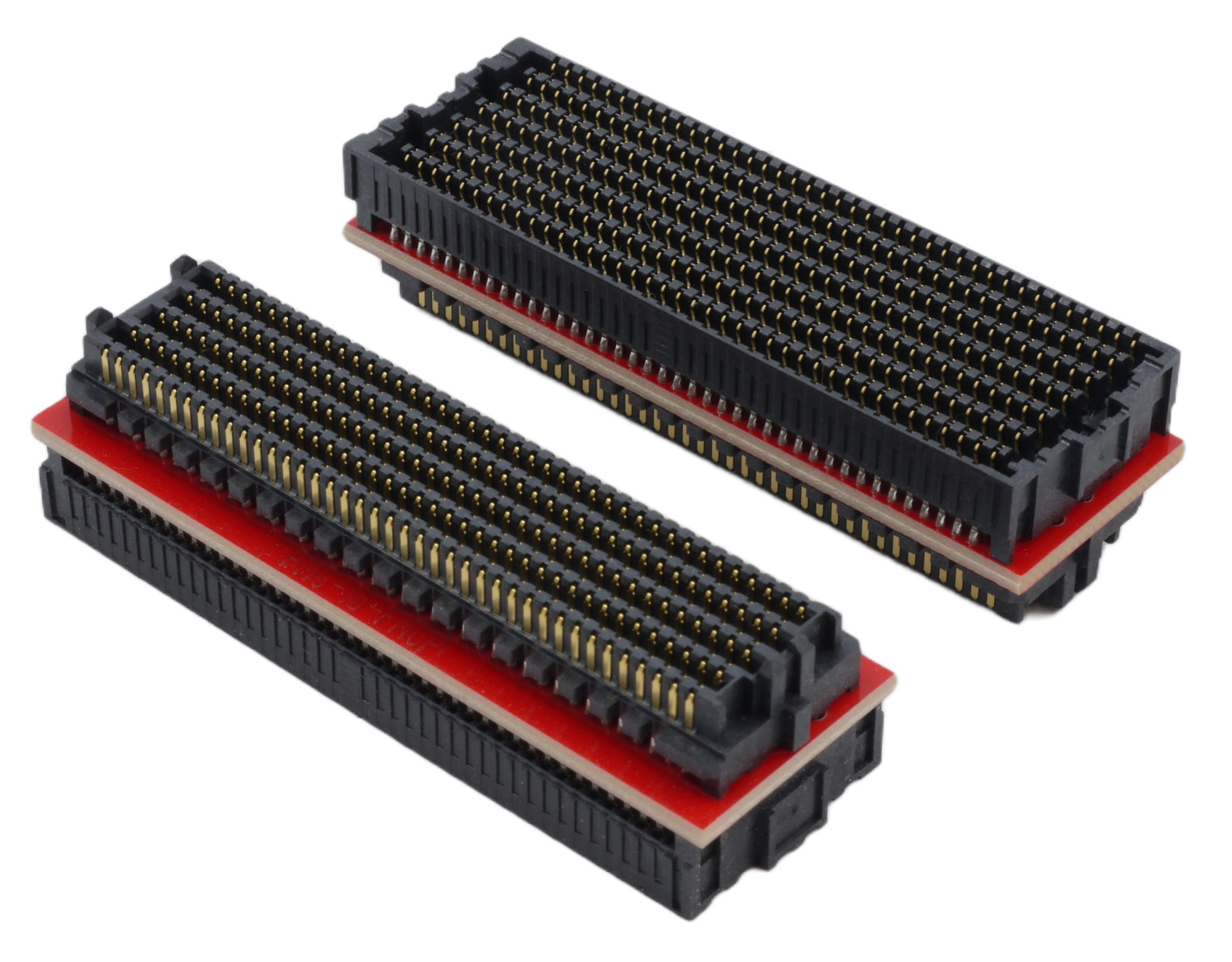

- Form Factor: FMC+ (VITA 57.4) to FMC (VITA 57.1) adapter
- High‑Speed Signaling: Designed for ultra‑high‑bandwidth data paths and validated in lab environments up to 12 Gbps per lane; electrical design and signal‑integrity margins support higher data rates depending on carrier and module capabilities
- Connector Mapping: Full FMC+ HPC pin‑mapping to FMC HPC, including LA/HA/HB pairs
- Clocking Support: Differential clock routing with low‑jitter paths optimized for high‑frequency operation
- Power Delivery: Regulated power rails with controlled impedance and filtering for sensitive analog/digital FMC modules
- I/O Compatibility: Supports high‑speed ADC/DAC modules, JESD204B/C devices, RF front‑ends, and digital I/O expansion cards
- Mechanical: Precision‑machined standoffs and alignment features for secure FMC module mounting
- Compliance: Follows VITA 57 signal‑integrity guidelines for high‑density mezzanine interconnects
This adapter was successfully used to interface two high‑speed ADC channels from the FMCP‑ADC3p0 FMC+ module with the SE120 carrier card, which provides a standard FMC connector. The extender maintained signal integrity across the FMC+/FMC transition, enabling reliable multi‑gigabit data capture in a mixed‑form‑factor setup.
Features
-
FMC+ to FMC Interoperability Enables seamless use of FMC modules on FMC+ carriers, extending the flexibility of FPGA prototyping platforms such as Xilinx, Intel, and SundanceDSP boards.
-
High‑Frequency Signal Path Optimization: The adapter has been tested at 12 Gbps lane speeds using high‑frequency signaling equipment. Trace geometry, via transitions, and reference‑plane design were engineered to maintain eye‑diagram integrity at multi‑gigabit rates. While validated at 12G, the board’s design supports higher data rates when paired with compatible FPGA carriers and FMC modules.
-
Low‑Loss PCB Stackup: Built using a controlled‑impedance, low‑loss laminate stackup to minimize attenuation and preserve signal fidelity for RF, JESD204, and high‑speed serial applications.
-
Robust Power & Grounding Architecture: Carefully partitioned power rails and ground return paths reduce noise coupling, making the adapter suitable for mixed‑signal FMC modules.
-
Ideal for Rapid Prototyping: Perfect for engineers needing to evaluate FMC modules on newer FMC+ platforms without redesigning hardware.
Applications
- FPGA development
- FPGA carrier card development
- FPGA carrier card used in test platform
- High-speed ADCs and DACs
- Next-generation RF connectivity
- High‑speed data acquisition
- RF and microwave prototyping
- JESD204B/C converter evaluation
- Real‑time signal processing
- Defense, aerospace, and instrumentation system
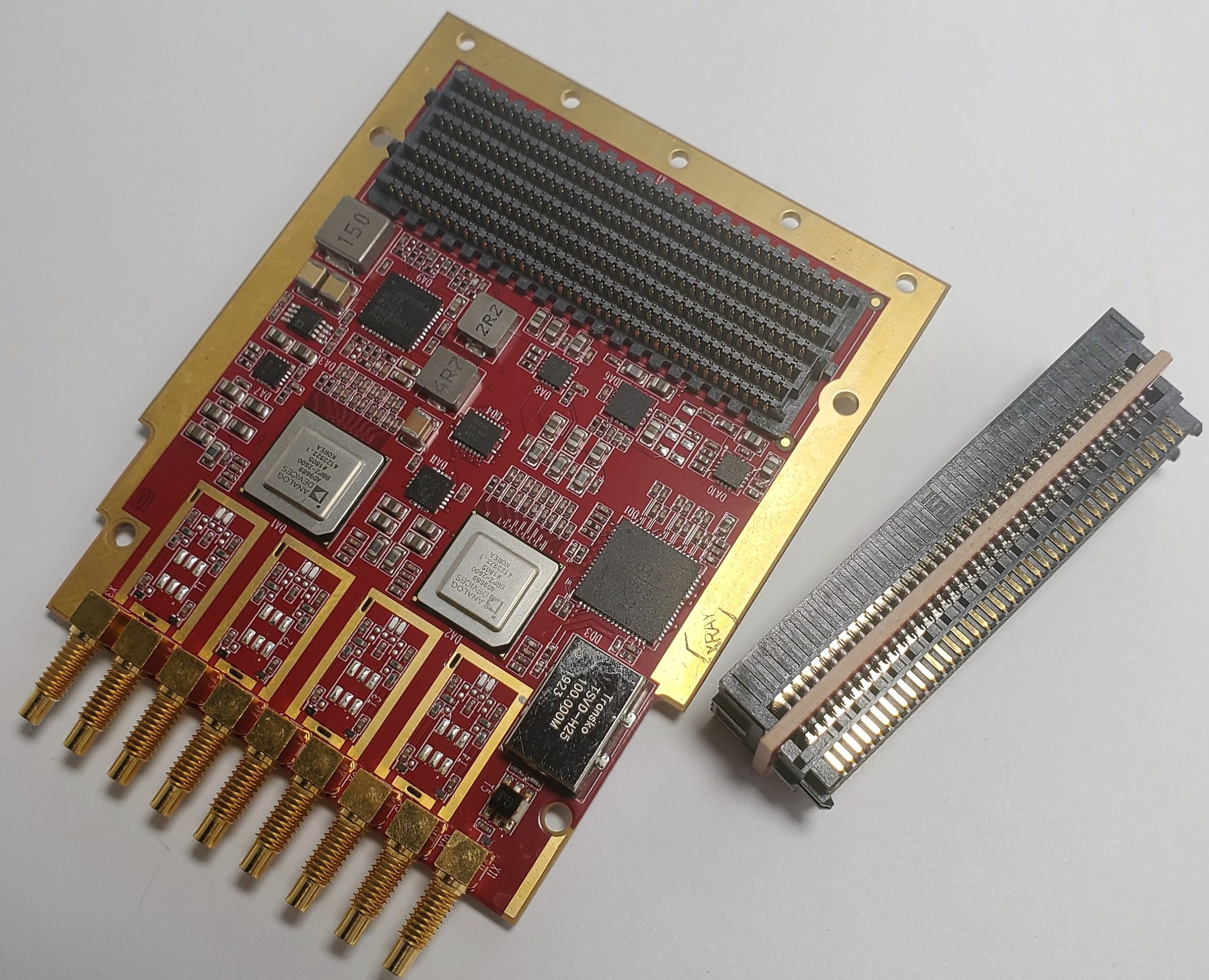
FMC-to-FMC+ converts FMC+ module to FMC