
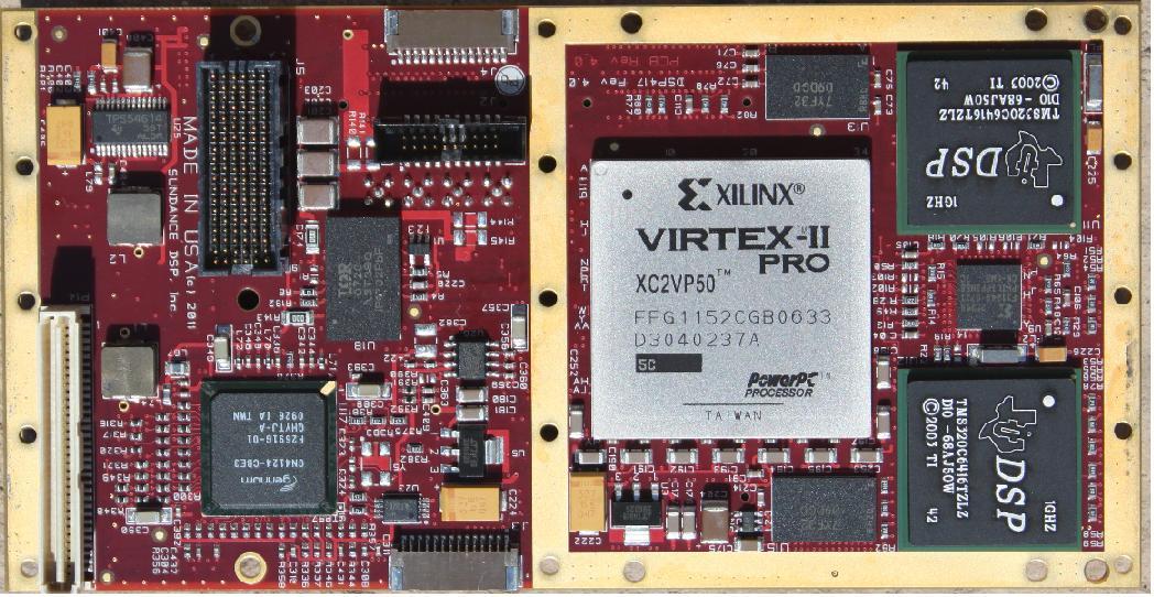

Dual TMS320C6416T TI DSP XMC / Standalone with x4 PCIe lanes
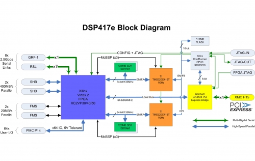
The DSP417e is a x4 PCIe module with a dedicated PCI Express bridge chip. This module provides a flexible platform for the next generation of Telecom systems, image processing applications, medical equipment and industrial solutions. With the added benefit of the large a Xilinx VirtexII-Pro.
(XC2VP50FF1152) FPGA, the DSP417 enables pre-processing to be done on-the-fly before the DSP gets the data. The Sundance-provided basic VHDL Core for inter-DSP communication uses 25% to 50% of the FPGA for I/O and system functions, while the rest is available for the user application.
A shared memory mechanism exists between the two DSPs on the DSP417e in addition to the inter-processor communication provided by comports and SHBs. DSP A has access to the memory space of DSP B.
There is also a large 512MB FLASH disk on the DSP417 which holds the boot loader as standard. This FLASH disk can be used for storing user application for booting from FLASH and also to store application data. This is particularly useful when one wants to store large amounts to data during a capture and then transfer to host or other devices later on.
The DSP417 was designed to be used in a conduction cooled environment, but it can be used also on a standard air environment.
Benefits
- Powerful processing module with FPGA resource
- Full multi-DSP software support from 3L Diamond
- Support for the TI Code Composer Studio
- Can be used in embedded systems
- Can interface to Sundance ADC, DAC, DSP, imaging and communications modules.
Features
- 4 lanes PCI Express interface with over 600MB/s data transfer to/from host
- 256MB of SDRAM
- 2 TI TMS320C6416T DSPs each @ 1GHz
- 2 Sundance High Speed Bus (SHB) interfaces
- Xilinx FPGA, Virtex II VP50
- 7 Rocket IO RSL interfaces
- IEEE 1386 standard PMC form factor with conduction cooling.
- 64bit / 66MHz PCI interface through PMC and 1 x8 or 2 x4 PCIe. through XMC
- Conduction cooled.
- XMC Connector per ANSI/VITA 42.0(42.2 for x4 RapidIO compatible).
- Supported by Diamond and PARS development software for multiprocessing.
- Large 512MB built in FLASH disk for storing applications and data.
- Shared memory architecture as well as inter-processor communication ports.
- Can cascade multiple DSP417es to build larger parallel systems.
- Can connect to low cost ADC and DAC modules from Xilinx.
- Over 600MB/s data transfer capability to/from host.
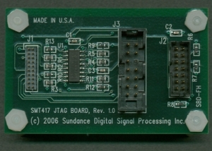
A JTAG daughter card is available for the DSP417. It provides standard interface to TI and Xilinx emulator cards. The JTAG interface can be used for firmware updates and/or software development.
DSP417e-VP50-x-y-z
x = B indicates 5V VPWR XMC
C 3.3V VPWR XMC
D 12V VPWR XMC
y = blank indicates no connectors on the back
E indicates all connectors on the back are fitted
z = blank indicates -5 speed grade FPGA (standard build)
F indicates -6 speed grade FPGA
Example product code:
DSP417e-VP50-B-F (faster -6 FPGA with no connectors on the back, with 5V VPWR XMC)