
Sundance DSP’s new fixed point FFT core combines performance and flexibility to offer an off-the-shelf product, which can be easily integrated into many applications. This product can be offered in both source and compiled version depending on the requirements.
Features
- With a generic and re-configurable architecture, the number of bits of input vector, number of butterfly processors and number of input and output points are easily changeable.
- By using a Pipeline structure, simultaneous input, parallel processing of most operations, and output (Triple memory FFT Processor) are ensured.
- 32 to 1024 points (or more) FFT Processors.
- Up to 32 input bits and up to 16 coefficients bits.
- Single, double and quad butterfly versions available.
- Fast operation, 100 clock cycles for 32 points single butterfly and 60 clock cycles for 32 points double butterfly. For instance, if a 32-point FFT core with only one Butterfly processor is used then 100 clock cycle are needed. For the same FFT with 2 butterfly processors the operation will take 60 cycles.
- The code is in RTL format and no primitives from Xilinx or any other vendor are needed.
A 32-point FFT example is described here to illustrate the operation of this IP core. A 32-point complex inputs with 2 butterfly processors is shown here. The core will receive 32 sets of complex fixed-point inputs serially and will calculate the FFT. Figure 1 depicts the computational architecture, comprising 5 columns and 16 rows. Here all processing is done with only butterfly processors a and b.
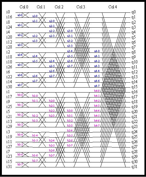 Figure 1: Buttefly and processor assignment for FFT Computation
Input and Output signals
| Signal Name | Mode | Description | Type | Bit Width |
| FClock | Input | Clock Signal | Bit | 1 |
| Reset | Input | Resets the circuit | Bit | 1 |
| Enable | Input | Denotes validity of input data | Bit | 1 |
| OutEn | Input | Shows output data maybe ready | Bit | 1 |
| InputR | Input | Real part of input data | Signed | N |
| InputI | Input | Imaginary part of input data | Signed | N |
| InFull | Output | Shows overflow in input buffer | Bit | 1 |
| OutReady | Output | Shows output data is ready to come out | Bit | 1 |
| DataValid | Output | Shows output bus has valid data | Bit | 1 |
| OutputR | Output | Real part of output data | Signed | N |
| OutputI | Output | Imaginary part of output data | Signed | N |
Timing Diagram
As shown in Figure 2, when Enable is active the input ports are supposed to be valid and the input vector is accepted in the input ports. After several clock pulses the output is ready and DataValid signal is activated.
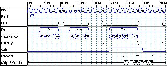 Figure 2: Input and Output timing diagrams
Synthesys and Timing Report
FFT Processor Core Specifications, Synthesized on Xilinx V1000E(-6) FPGA
| FFT Points | Butterfly Units | Input Bits | Precision Bits | Operation Clock Cycles | FPGA | Freq MHz | Operation Time (us) | CLBs | Flip Flops | Memory Bits |
| 32 | 1 | 16 | 10 | 100 | V1000E | 65 | 1.538 | 1424 | 1465 | 2.5k |
| 64 | 1 | 16 | 10 | 216 | V1000E | 63 | 3.428 | 1485 | 1545 | 5k |
| 128 | 1 | 16 | 10 | 476 | V1000E | 64 | 7.437 | 1564 | 1642 | 10k |
| 256 | 1 | 16 | 10 | 1056 | V1000E | 63 | 16.761 | 1583 | 1711 | 20k |
| 512 | 1 | 16 | 10 | 2340 | V1000E | 59 | 39.661 | 1671 | 1784 | 40k |
| 1024 | 1 | 16 | 10 | 5160 | V1000E | 59 | 87.457 | 1762 | 1860 | 80k |
| 32 | 2 | 16 | 10 | 60 | V1000E | 62 | 0.967 | 2989 | 2834 | 2.5k |
| 64 | 2 | 16 | 10 | 120 | V1000E | 62 | 1.935 | 3114 | 2992 | 5k |
| 128 | 2 | 16 | 10 | 252 | V1000E | 62 | 4.064 | 3275 | 3174 | 10k |
| 256 | 2 | 16 | 10 | 544 | V1000E | 61 | 8.918 | 3275 | 3309 | 20k |
| 512 | 2 | 16 | 10 | 1188 | V1000E | 57 | 20.842 | 3467 | 3456 | 40k |
| 1024 | 2 | 16 | 10 | 2600 | V1000E | 54 | 48.148 | 3603 | 3591 | 80k |
| 32 | 4 | 16 | 10 | 40 | V1000E | 60 | 0.666 | 6626 | 5521 | 2.5k |
| 64 | 4 | 16 | 10 | 72 | V1000E | 59 | 1.220 | 6893 | 5829 | 5k |
| 128 | 4 | 16 | 10 | 140 | V1000E | 59 | 2.372 | 7239 | 6190 | 10k |
| 256 | 4 | 16 | 10 | 288 | V1000E | 50 | 5.76 | 7292 | 6447 | 20k |
| 512 | 4 | 16 | 10 | 612 | V1000E | 51 | 12 | 7765 | 6751 | 40k |
| 1024 | 4 | 16 | 10 | 1320 | V1000E | 49 | 27 | 8031 | 7024 | 80k |
FFT Processor Core Specifications, Synthesized on Xilinx V1000E(-8) FPGA
| FFT Points | Butterfly Units | Input Bits | Precision Bits | Operation Clock Cycles | FPGA | Freq MHz | Time (us) | CLBs | Flip Flops | Memory Bits |
| 32 | 1 | 16 | 10 | 100 | V1000E | 87 | 1.15 | 1424 | 1465 | 2.5k |
| 64 | 1 | 16 | 10 | 216 | V1000E | 84 | 2.57 | 1485 | 1545 | 5k |
| 128 | 1 | 16 | 10 | 476 | V1000E | 85 | 5.6 | 1564 | 1642 | 10k |
| 256 | 1 | 16 | 10 | 1056 | V1000E | 84 | 12.57 | 1583 | 1711 | 20k |
| 512 | 1 | 16 | 10 | 2340 | V1000E | 78 | 30 | 1671 | 1784 | 40k |
| 1024 | 1 | 16 | 10 | 5160 | V1000E | 78 | 66.15 | 1762 | 1860 | 80k |
| 32 | 2 | 16 | 10 | 60 | V1000E | 83 | 0.723 | 2989 | 2834 | 2.5k |
| 64 | 2 | 16 | 10 | 120 | V1000E | 83 | 1.466 | 3114 | 2992 | 5k |
| 128 | 2 | 16 | 10 | 252 | V1000E | 83 | 3.036 | 3275 | 3174 | 10k |
| 256 | 2 | 16 | 10 | 544 | V1000E | 81 | 6.716 | 3275 | 3309 | 20k |
| 512 | 2 | 16 | 10 | 1188 | V1000E | 76 | 15.63 | 3467 | 3456 | 40k |
| 1024 | 2 | 16 | 10 | 2600 | V1000E | 72 | 36.11 | 3603 | 3591 | 80k |
| 32 | 4 | 16 | 10 | 40 | V1000E | 80 | 0.5 | 6626 | 5521 | 2.5k |
| 64 | 4 | 16 | 10 | 72 | V1000E | 78 | 0.923 | 6893 | 5829 | 5k |
| 128 | 4 | 16 | 10 | 140 | V1000E | 78 | 1.795 | 7239 | 6190 | 10k |
| 256 | 4 | 16 | 10 | 288 | V1000E | 67 | 4.3 | 7292 | 6447 | 20k |
| 512 | 4 | 16 | 10 | 612 | V1000E | 68 | 9 | 7765 | 6751 | 40k |
| 1024 | 4 | 16 | 10 | 1320 | V1000E | 65 | 20.3 | 8031 | 7024 | 80k |
Devices
- Xilinx Virtex-II, Virtex-II Pro, Virtex-4. Amongst Sundance modules, this can be implemented on:
- SMT398 (Virtex II and ZBT SRAM)
- SMT338-VP (Virtex-II pro and DDR SDRAM)
- SMT398-VP (Virtex-II pro and QDRII SDRAM)
- SMT368 (Virtex-4 and ZBT RAM)