


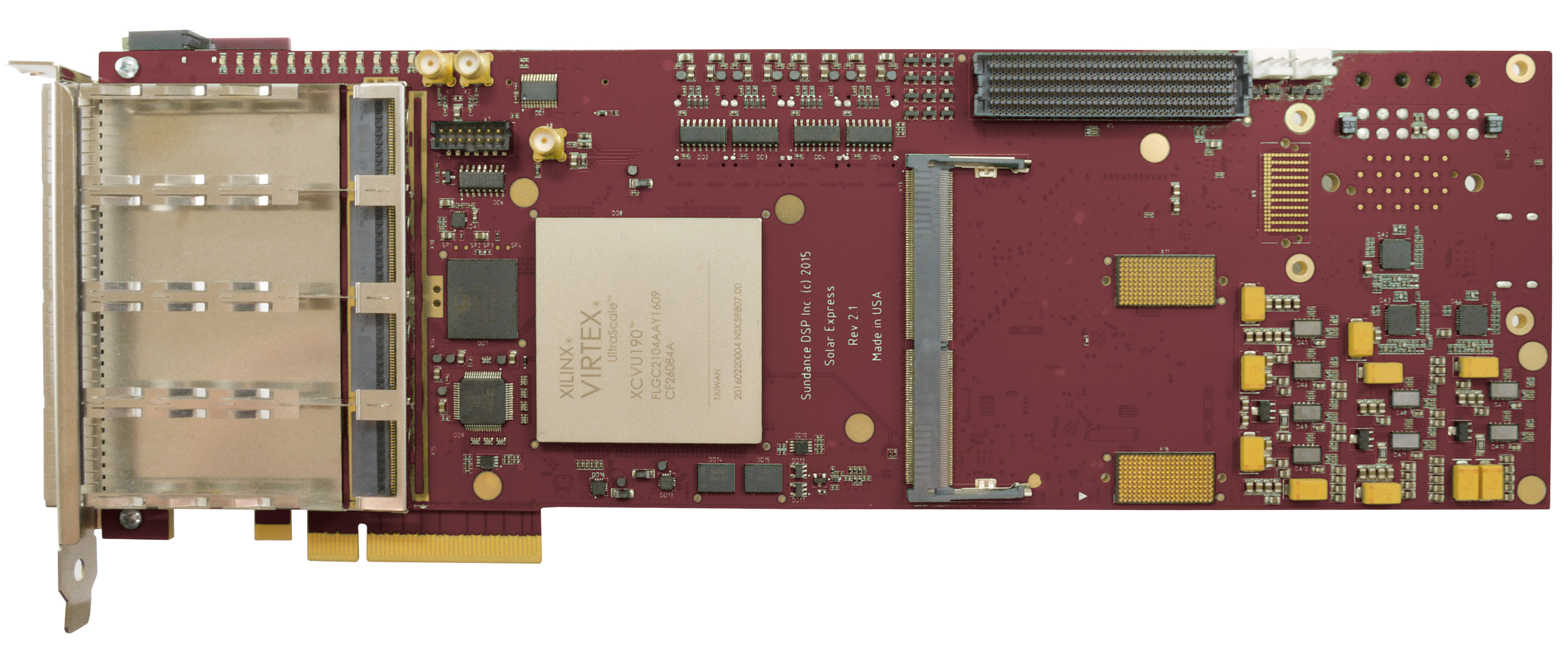
SE100 is based on Xilinx’s Virtex Ultrascale FPGA XCVU190-2FLGC2104E, and is a powerful processing card with plenty of IO capabilities to meet the needs of modern compute-intensive applications such as Supercomputing, Data Centers and defense. The board can optionally be populated with 095, 125, and 160 devices in C2104 package for reduced cost. Host interface is via 8 lanes of PCIe Gen3 but the card can also be used as an embedded, standalone, hardware too. Multiple cards can be cascaded to provide a multi-FPGA system with cards connected together via the board’s fast IO channels to meet the needs of even more demanding applications like ASIC design and Stock Market fast trading systems.
SE100 offers a host of features such as CFP4 to support high speed optical networking, data communication and processing.
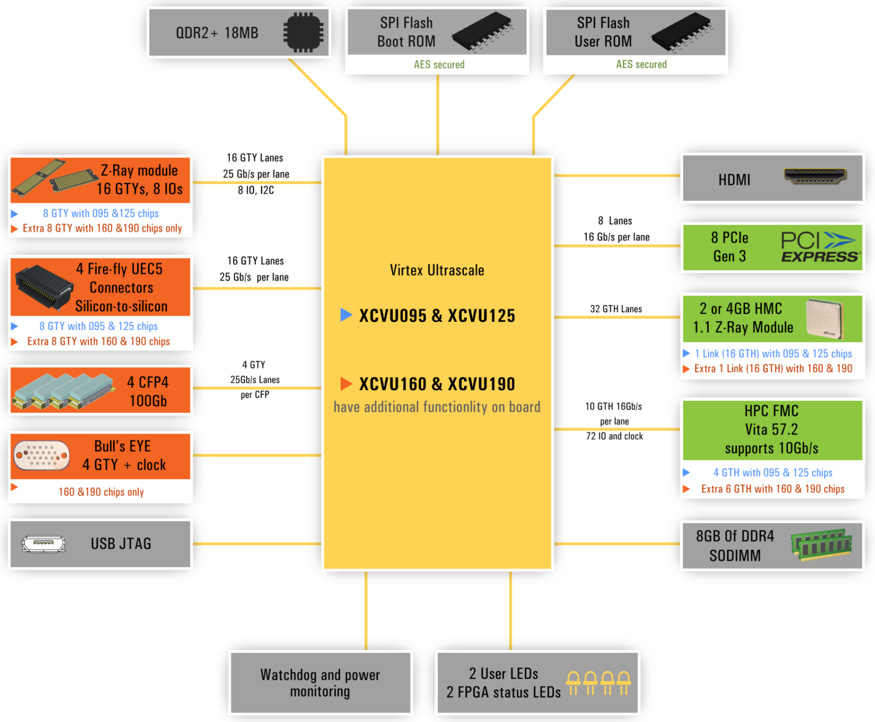
Solar Express 100 features additional I/O expansion options using the latest high-speed board-to-board connectors from Samtec. The HPC FMC interface offers 10 GTHs (16.3Gb/s) and 40 IOs. Multiple Samtec Z-Ray® interposers provide access to an HMC modules and additional 16 GTY transceivers (16 x 30.5Gb/s) and 8 IO plus 12V/5A, 3.3V/16A, and VCCIO/1A. A 2GB HMC memory module with 4 links (8 GTH per link) offering concurrent access can be added. This will enable fastest memory access by the FPGA. 18MB of “QDR2+” memory comes as standard and 8GB of DDR4 can be added as a SODIMM.
One Samtec Bull’s Eye® Test Point System provides access to additional 4 GTY transceivers.
The board also includes 4 Samtec FireFly™ Micro Flyover System™ interfaces where each provides copper or optical silicon-to-silicon connectivity via 4 GTY transceivers.
FireFLy is protocol agnostic and supports all data center applications and HPC protocols including Ethernet, InfiniBand™, Fiber Channel, and PCIe.
For details of FireFly cable options please contact SDSP technical support team.

An HDMI port codec allows direct display of images, with suitable IP core, while 4xGTYs and clock on a Samtec Bull’s Eye connector gives more flexibility for data import/export.
Features
- Virtex Ultrascale FPGA XCVU190-2FLGC2104E (other options available)
- x8 lanes PCIe Gen3 (Gen4 with soft core)
- x2 lanes PCIe104 PCIe Gen3 connector
- Up to 1600 Mbps LVDS signaling
- Up to 1250 Mbps single ended (standard I/O)/
- Up to 16.375Gbps each for the 52 GTHs transceivers and 28.21Gbps each for the 48 GTY tranceivers (speed grade-2, and to 30.5Gbps for speed grade-3)
- 1 FMC expansion site with up to 10 GTH 16.3Gb/s transceivers and 40 single ended IOs and 4 GPIO
- FMC module auto detection and adjustment of right voltage through IP core
- ZRay expansion site 1 (x1 ZRay connector) with 16GTY (30.5Gb/s per transceivers), 8GP IOs supporting 1V8 to 3V3 for control, I2C bus and power.
- ZRay module site 2 (x2 ZRay connector) for connecting Sundance HMC ZRay module (or other modules) with 2GB of memory. Has 32 GTHs, control IO and power with 1V8
- 18MB of QDR2+ memory
- Upto 16 GB of SDRAM via DDR4 SODIMM
- Quad CFP4 with 100Gb/s each, for optical networking (can have additional 100Gb/s interfaces through FireFly and ZRay module.
- 4 GTYs and clock available on Samtec Bull’s Eye
- 4 FireFly connector each with 4 GTYs delivering 400Gb/s aggregate, full duplex
- HDMI interface codec
- Flash memory for user application bitstream
- JTAG through USB2.0 connector
- Capability to reconfigure FPGA from host PCIe
- System monitoring
Applications
- Data Analytics
- Network Acceleration
- Data Centers
- Digital Communications
- High performance optical networking
- High-end Image Processing
- ASIC/SOC prototyping and development
- Machine Vision
- Machine Learning
- Intelligence and security,
- Mega performance computing
- High Frequency/Speed stock trading
- Defense
3D image of the SE100 with heat sink
 |
|
 |
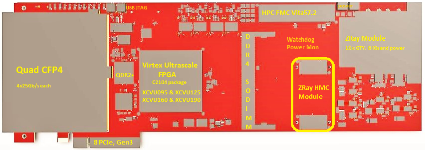 |
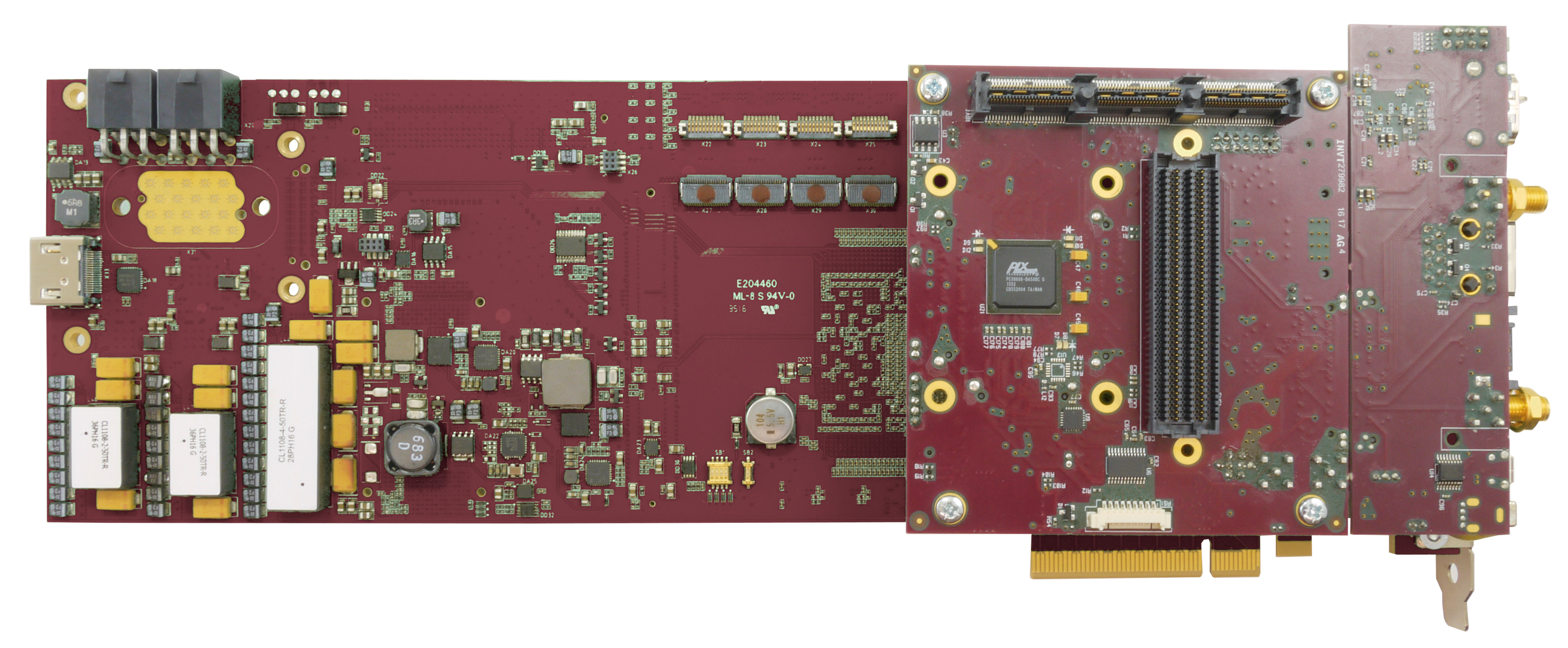
| SE100 without heat sink | with heat sink | solder side with attached EMC2 PCIe104 | Location of major modules |
Block Diagram
Summary of devices and available resources:
| Device Name | XCVU095 | XCVU125 | XCVU160 | XCVU190 |
| Effective LEs(1) (K) | 1129 | 1504 | 1945 | 2256 |
| Logic Cells (K) | 941 | 1253 | 1621 | 1880 |
| Total Block RAM (Mb) | 60.8 | 88.6 | 115.2 | 132.9 |
| I/O DLL | 64 | 80 | 120 | 120 |
| DSP Slices | 768 | 1200 | 1560 | 1800 |