
The Solar Express 2000 (SE2000) is a 3U SOSA-aligned OpenVPX PIC card based on the AMD Versal ™ AI Edge and Prime Gen 2 devices (The choice between an AI Edge or Prime device is an ordering option, the first available SE2000 module comes with a Versal AI Edge Series Gen 2 device in an SSVA2112 package, XC2VE3858-2MSISSVA2112; other devices will become available over time).
The board is suitable for high-speed data processing, analysis, and AI inferencing.
This VPX board has many advanced features, including optical and RF interfaces and an FMC+ connector for additional flexibility and expandability. It comes with an AMD Artix™ FPGA, which acts as a voltage translator between the AMD Versal and the FMC+ connector supporting the traditional voltages offered by FMC+ modules.
The board is designed for defense, aerospace, and research applications and is made in USA.
Download datasheet
Features
The hardware will have the following features:
- Board form factor and Profile, SOSA compatible: MOD3-PAY-1F1U1S1S1U1U2F1H-16.6.11-x
- SOSA slot profile SLT3-PAY-1F1U1S1S1U1U2F1H-14.6.11-6 (other “dash” options are supported — contact Sundance support for more information)
- IPMC: STM32L433RCI6 microcontroller
- Main payload devices available as ordering options:
SSVA2112 package, Versal AI Edge Gen2 2VE3504, 2VE3558, 2VE3804, 2VE3858, Versal Prime Gen2 2VM3558, 2VM3858 - GTYP, GTM resource allocation:
GTYP(PL) – 12 (Max 20), GTYP(PS) – 4, X5IO – 384 (Max 512) (SSVA2112 package) - 16 GB eMMC for PS image and data storage (can populate up to 256 GB)
- Two 1 GB QSPI flash for PS image and data storage
- TA101 Secure authentication IC connected to PS for secure boot and encryption capabilities
- TPM 2.0 for storage of encryption keys for the PS, ST33HTPH2X32AHE4
- Si5341 Clocking IC (10 outputs, low jitter)—provides fabric clocks and transceiver clocks
- FT4232 USB-to-UART: provides 3 UART channels (payload PS, payload PL, IPMC) and JTAG (including FMC+) via USB Type-C connector
- DIP switches for JTAG bypass, boot-mode selection, and user purposes
- Two RGB LEDs (one connected to PS, one to PL)
- IPMC SWD JTAG routed to the OpenVPX connector
- Combined MicroSD/UFS card connector—boot capable (microSD supports only 3.3 V modes)
- Maintenance ports routed to IPMC and to Payload PS UART
- Redrivers on Data, Control, Expansion plane signals:
PI3EQX16904GLZHEX (Expansion plane), PI3EQX1204-CZHEX (other planes) - Optical module with 12 Tx and 12 Rx lanes (to build 3×100 Gb Ethernet ports)
- There is constant GTYP routing not controlled by assembly option, not subject to change:
- PS GTY_Q_105 — routed to Expansion Plane EP00–EP03 (PCIe only)
- 4× PL GTYPs[00:03] — routed to Data plane 1
- There are stuff resistors for different assembly options, routing GTYPs to different interfaces:
- For devices with 12 GTYPs:
- 4× GTYPs[04:07] — FMC+ DP[00:03] or Optical
- 2× GTYPs[08:09] — FMC+ DP[04:05] or Optical
- GTYP[10] — FMC+ DP[06], Optical, or DPutp01
- GTYP[11] — FMC+ DP[07], Optical, or CPutp01
- For devices with 20 GTYPs:
- 4× GTYPs[08:11] — FMC+ DP[04:07] or Optical
- 4× GTYPs[12:15] — FMC+ DP[08:11] or Optical
- GTYP[16:17] — FMC+ DP[12:13]
- GTYP[18] — DPutp01
- GTYP[19] — CPutp01
- For devices with 12 GTYPs:
- Voltage & current sensing IC for the 12 V rail only, connected to IPMC and Payload via SMBus (other rails provide PG signal only)
- Temperature sensing IC connected to IPMC via I²C
- Onboard power control per OpenVPX specification, via IPMC
- Requires chassis 12 V supply and 3.3 V AUX supplies
- Enclosure compliance: VITA 48.2 conduction cooling and VITA 48.8 air cooling
- IPMC features:
- NVMRO signal processing
- IPMA, IMPB ports routed
- PMBus access with power & temperature sensors
- SWD JTAG routed from OpenVPX connector to IPMC
- Maintenance port from OpenVPX connector to IPMC
- GDiscrete1, GPIO1, MASK_RESET#, VPX_SYSCON#, GA[0:4], GAP routed to IPMC
- Early 3.3 V AUX warning
- Payload power control
- Internal PG signals
- IPMC to Payload connections & features (air-gappable):
- 1 SPI interface
- 9 GPIOs and 1 RESET#
- OpenVPX signals (GDiscrete1, SYS_CON#, GPIO1, MASK_RESET#) can route directly to Payload via resistor stuff option
- XC7A15T-1FGG484I FPGA for FMC LA/HA lanes level translation
- FMC+ VADJ voltage support: 1.8 V, 2.5 V, 3.3 V
- Maximum power draw: 200 W (TBD) from 12 V rail
Applications
- AI inferencing
- Defense
- Medical
- Imaging
- Software Defined Radio
|
 |
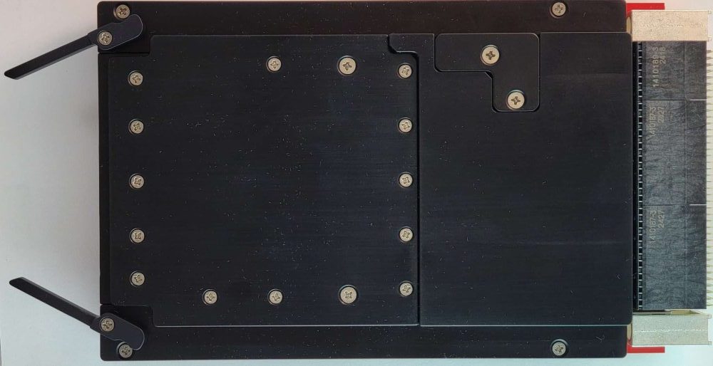 |
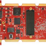
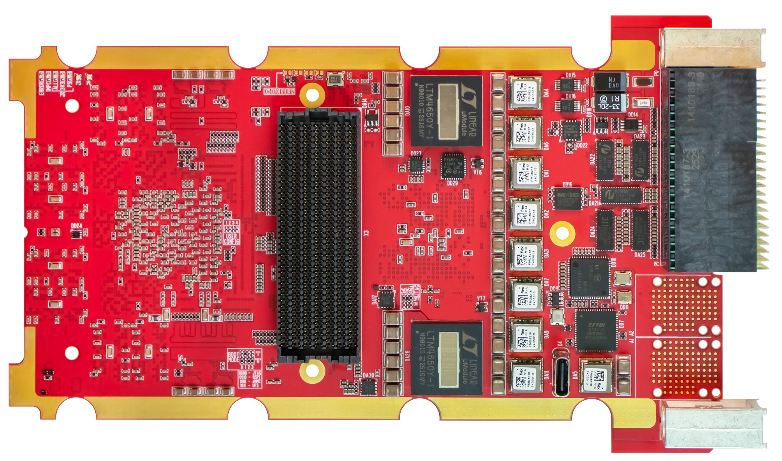
| SE2000 Back | SE2000 Front | SE2000 Versal-VPX with enclosure |
Block Diagram
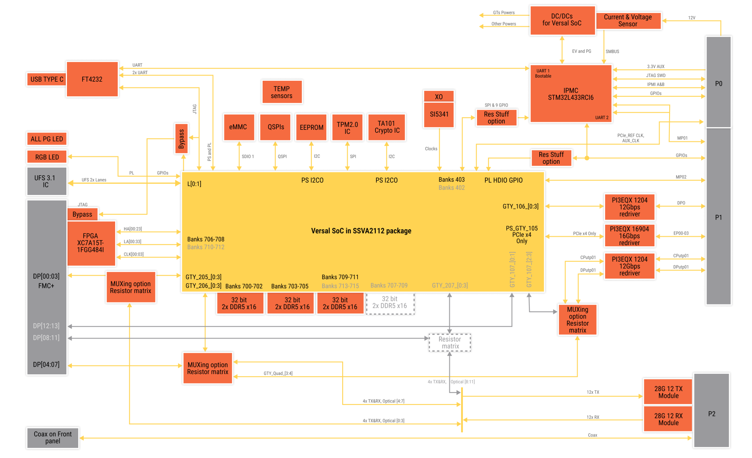
SE2000, Versal-VPX , SOSA aligned, block diagram
A complete BSP with Linux driver will be supplied.
SE2000-xxxxxxx-yy where “xxxxxxx” can be any of the options in Table 1: AMD Payload Options and “yy” can be any of the -n P2 connectors options shown in the Table 2: P2 Connector Options below
Table 1: AMD Payload Options
| AMD Device option | Description |
| 2VE3504 | AMD Versal ™ AI Edge Gen 2 2VE3504 in SSVA2112 package, 12GTYP XCVRs, 4APU cores, 4RPU cores, AIE-ML v2 |
| 2VE3558 | AMD Versal ™ AI Edge Gen 2 2VE3558 in SSVA2112 package, 12GTYP XCVRs, 8APU cores, 10RPU cores, AIE-ML v2 |
| 2VE3804 | AMD Versal ™ AI Edge Gen 2 2VE3804 in SSVA2112 package, 20GTYP XCVRs, 4APU cores, 4RPU cores, AIE-ML v2 |
| 2VE3858 | AMD Versal ™ AI Edge Gen 2 2VE3558 in SSVA2112 package, 20GTYP XCVRs, 8APU cores, 10RPU cores, AIE-ML v2 |
| 2VM3558 | AMD Versal ™ Prime Gen 2 2VM3558 in SSVA2112 package, 12GTYP XCVRs, 8APU cores, 10RPU cores |
| 2VM3654 | AMD Versal ™ Prime Gen 2 2VM3558 in SSVA2112 package, 20GTYP XCVRs, 4APU cores, 6RPU cores |
| 2VM3858 | AMD Versal ™ Prime Gen 2 2VM3558 in SSVA2112 package, 20GTYP XCVRs, 8APU cores, 10RPU cores |
| -TBD | Other options may be supported. Please contact Sundance DSP support for more information |
Table 2: P2 Connector Options
| “-n” option | Description |
| -0 | No P2 connector installed |
| -6 | 2 Style C and 10 NanoRF |
| -12 | 2 Style C and 20 NanoRF |
| -14 | 2 Style D |
| -TBD | Other options may be supported. Please contact Sundance DSP support for more information |
Early Access board will be SE2000-2VE3858-0
Early access to this board can be granted to interested customers, but the estimated delivery for prototype version will be Q4 of 2025.
Additional speed grades and temperature grades will become available as new parts are released. “-2MSI” speed and industrial temperature grade is default.