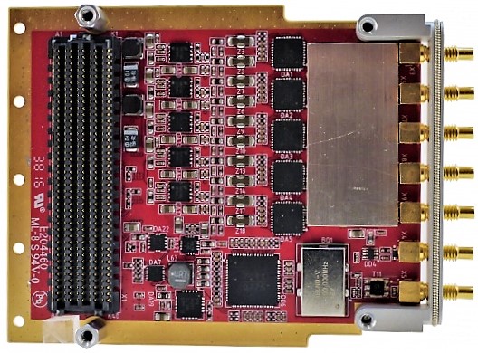
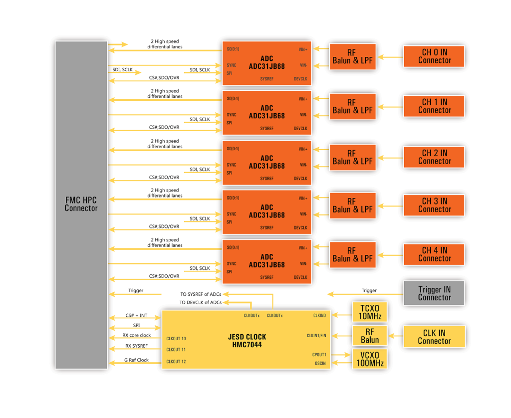
FMC-ADC500-5 is a High Pin Count (HPC) FMC module with 5 ADC channels, each channel running up to 500MS/s with a dynamic range of 16 bits. The module has 5 ADC31JB68 ICs from Texas Instruments in total with an HMC7044 from ADI, which is the source of clocks feeding the ADCs. We provide the provision for external clock input for this hardware.
An internal VCXO and TCXO clock are the input to HMC7044 with five clock outputs to the ADCs. HMC7044 offers an SYSREF clock with a known and adjustable delay, which can be sent to the FPGA as REF CLK and SYSREF CLK to achieve the requirement of subclass 1 JESD204B. The external clock input can be used as a Device clock for ADCs or as a reference clock.
ADC input signal bandwidth is 4.5 to 250MHz, while the external clock bandwidth is 10 to 800Mhz when used as a reference clock, and 400 to 4000Mhz when used as a device clock. Trigger maximum voltage will be 6V on this module.
External trigger input allows the addition of timestamps to the sample stream from ADCs. CLK IN can be a Sample clock input up to 4GHz or reference clock input up to 800MHz. Board clocking structure provides the possibility of deterministic latency and subclass one synchronization between multiple ADCs.
ADC Parameters
- 16-Bit Resolution, single-Chanel, 500MSPS ADC
- INL: ±7.1 LSB (Ta = 25)
- DNL: ±0.23 LSB (Ta = 25)
- Spectral Performance (fIN = 210 MHz at –1 dBFS):
- SNR: 69.3 dBFS
- NSD: –153.3 dBFS/Hz
- SFDR: 80 dBFS
- ENOB: 11.3 Bits
- Spectral Performance (fIN = 10 MHz at –1 dBFS):
- SNR: 70.3 dBFS
- NSD: –154.3 dBFS/Hz
- SFDR: 83 dBFS
- ENOB: 11.3 Bits
- Input Full-Scale differential: 1.7 VPP
- Full power Bandwidth: 1300 MHz* NOTE: Input Bandwidth limited to 250 MHZ, due to anti-alias filter
Clock and trigger-in parameters
- External clock in the frequency range, in reference clock mode – 10 – 800MHz
- External clock in the frequency range, in device clock mode – 400 – 4000MHz
- Input: AC coupled, 50 Ohm, single-ended.
- Input power range: -6 to 6 dBm.
- Trigger input – logic level, ESD protected, LVTTL 3.3V
Features
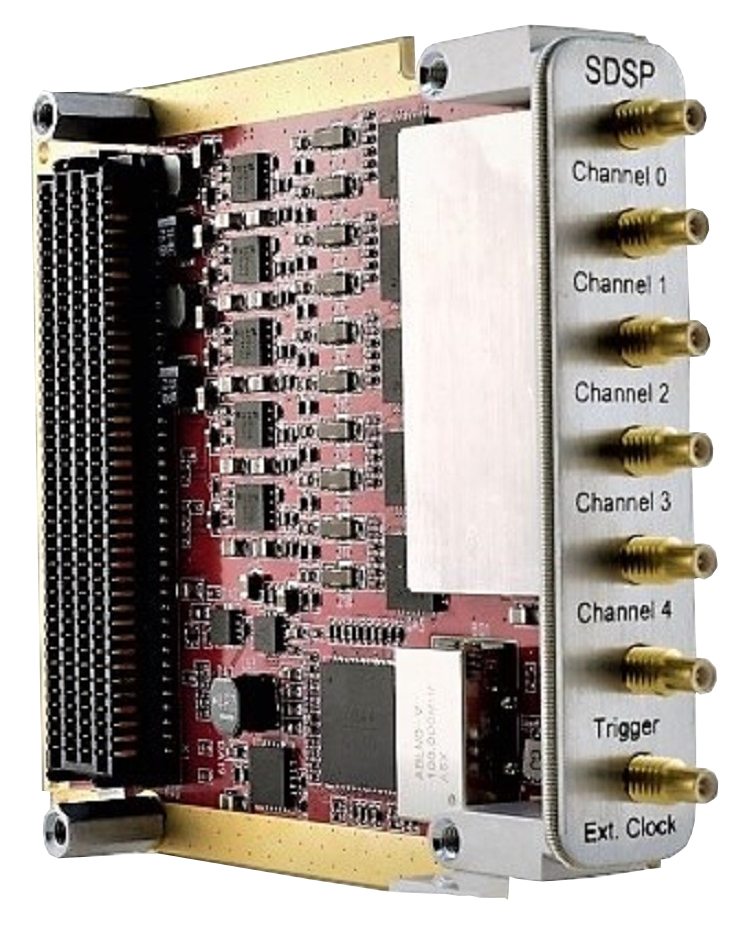
- 5 x ADC 16 bit @ 500MS/s
- High Pin Count ( HPC ) FMC module
- Trigger Input
- External Clock up to 4 GHz
- 100 MHz onboard VCXO and 10MHz TCXO for reference clock
- Compliant with JESD204B subclass 1
- Time stamp with external trigger
- Deterministic delay
- Vadj voltage support for 1.8, 2.5 and 3.3V
- Commercial and Industrial grades
- x8 SSMC RF JACK connector, part number 7110-1511-000
Applications
- Radar / Sonar
- Wireless communication transceivers / base stations
- Defense / Aerospace / Satellite communications
- Medical
- Automotive
- Direct RF Down Conversion
- Test and measurement
- Beamforming / Directional vector
- Software-defined radio (SDR)
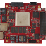
Frontal view of FMC-ADC500-5
This module can be expanded/pipelined using additional FPGAs cards if necessary.
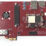
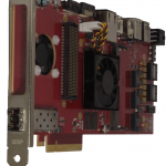
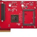
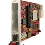
FMC-ADC500-5 is supported by Sundance DSP PXIe700, PXIe, and PCIe FPGA boards using the Xilinx Kintex series. Our PXIe700 and PCIe-K800 are 100% user-programmable with an open FPGA that enables users to implement their proprietary signal pre-processing algorithms