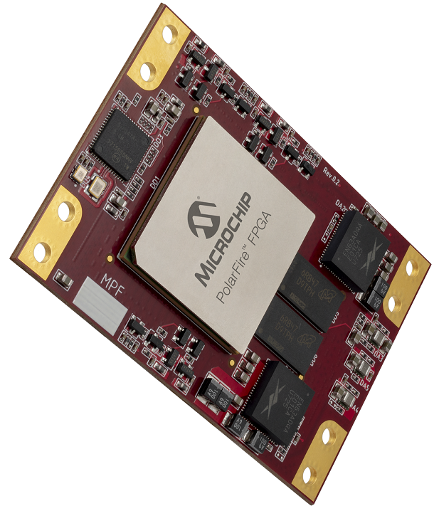
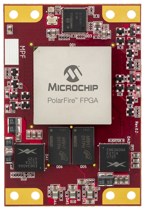
SoM2 is a System on a Module using the powerful, low-power, and high-security PolarFire FPGA from Microsemi. It is based on the MPF300T-1FCG784E FPGA with a small footprint, low power and high security. With its relatively low cost, it can be suitable for applications where pricing is important. The module includes 4GB of DDR4 memory at 1600Mb/s. The use of Sundance SOMs in your design can remove much complexity from the development and increases the success rate and decreases time to market. The module is compatible with some SoMs from Trenz and can be used on their SOM carrier card. PolarFire FPGAs offer design security with transceivers, low power transceiver devices, data security with transceivers, and low power data security with transceiver devices. All PolarFire FPGAs are integrated with multi-protocol industry-leading low-power transceivers. Low power (L) devices provide up to 35% lower static power. Also, data security (S) devices have an integrated DPA-safe crypto accelerator. PolarFire Devices are currently offered in Extended Commercial (0ºC to 100ºC) and Industrial (–40ºC to 100ºC) device offerings. The Libero SoC PolarFire Design Suite delivers a number of many soft IP cores, including a RISC-V processor, Data Security, Ethernet, DES encryption, error detection and correction, and more. This helps kick start many development projects and reduces time to market.
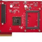
SE200 PCIe SOM carrier can be sued for development or as an embedded carrier.
SOM2 and SOM1 have a small footprint of 76 x 52 mm.
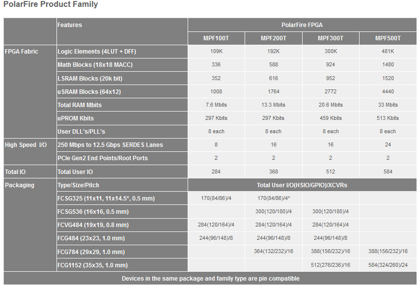
For reference here is the resource and available packages of Polar Fire and please note that parts in the same package are pin compatible.
Features
- PolarFire MPF300T-1FCG784E FPGA orMPF300T-1FCG784E,or MPF500T-1FCG784E FPGA
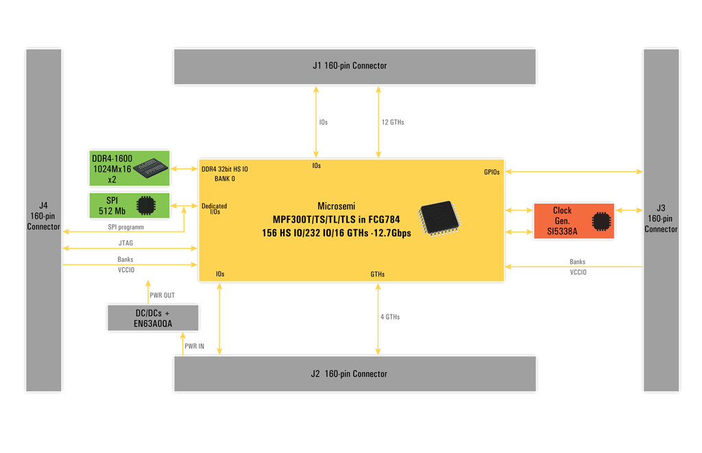
- Two MT40A1G16 memory chips from Micron(stacked 2 x8 8Gb chips) – total 32Gbits (4GB) of DDR4-1600 (effective data lanes’ speed of DDR4 interface reduced to 1600Mb/s – clock rate maximum 800MHz)
- 512Mbit SPI Flash for bitstream and other code storage, by default, the flash will not be soldered;
- Flexible clocking IC – SI5338A-B-GM with 50MHz ±20ppm reference oscillator;
- Built-in FPGA internal oscillator for configuration and other purposes;
- B2B Connectors: 4 x 160 Pins from Samtec – ST5-80-1.50-L-D-P-TR;
- I/O’s – from Banks; MAX LVDS I/O speed is 1600Mbps
- High-speed transceivers; maximum speed is 12.7Gbps
- Input power supply for the module;
- Separate pins for VCCIO supply;
- Flexible clocking scheme.
- The small footprint of 76 x 52 mm.
- Temperature range 0°C to +65°C;
- Power IN from 3.3V to 5.5V.
- Max FPGA power consumption is below 10 Watts
- Temperature range 0°C to +65°C;
Applications
- Defense
- Communications
- Industrial
- Machine automation
 |
 |
|
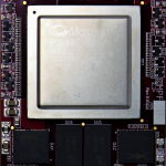
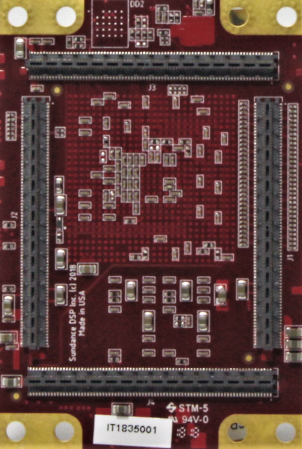
| Component side | Solder side | SoM2 on SE200 Carrier |
Block Diagram
SoM2-MPF200-1-E -1 speed grade with an MPF200T-1FCG784E FPGA and with 4GB of DDR4 memory
SoM2-MPF300-1-E -1 speed grade with an MPF300T-1FCG784E FPGA and with 4GB of DDR4 memory
SoM2-MPF500-1-E -1 speed grade with an MPF500T-1FCG784E FPGA and with 4GB of DDR4 memory
For Industrial grade part please order:
SoM2-MPF200-1-I
SoM2-MPF300-1-I
SoM2-MPF500-1-I