
Specifications
The PCIe104Z is a high-performance embedded computing board built around the Xilinx Zynq UltraScale+ MPSoC in a C1156 package (FFVC1156E for select variants), offering a range of processor options to suit different computational demands, power budgets, and environmental conditions. These variants offer a hybrid architecture that combines multi-core ARM processors for general-purpose computing with a programmable logic (PL) fabric for hardware acceleration, alongside integrated features such as real-time processing units, memory controllers, and high-speed interfaces.
All variants include a dual-core ARM Cortex-R5 real-time processor unit (up to 600MHz with ECC-protected memory) for deterministic control tasks, support for dynamic memory interfaces (DDR4), static memory interfaces (eMMC, Quad-SPI), and general connectivity options such as USB, SATA, DisplayPort, Gigabit Ethernet, UART. They are available in industrial-grade configurations, supporting operating temperatures from -40°C to 100°C (extended to 110°C in some cases) for the Zynq device, ensuring reliability in harsh environments such as outdoor deployments, industrial automation, or aerospace applications where vibration, shock, and thermal extremes are common.
Key variants include:
- XCZU7EV-2FFVC1156E: Features a quad-core ARM Cortex-A53 application processor (up to 1.5GHz with L1/L2 caches and ECC) paired with a Mali-400 MP2 graphics processing unit (up to 667MHz), speed grade of -2, and extended temperature range. It is uniquely integrated with a dedicated Video Codec Unit (VCU) supporting H.265/H.264 encoding/decoding at up to 4K resolution, enabling efficient video processing for bandwidth-constrained applications like streaming or compression.
- XCZU7EG: Quad-core ARM Cortex-A53 (up to 1.5GHz with caches and ECC) with Mali-400 MP2 GPU (up to 667MHz), speed grade -2, extended temperature. This variant offers balanced performance for graphics-accelerated tasks without the specialized video codec, making it suitable for general embedded computing.
- XCZU11EG: Quad-core ARM Cortex-A53 (up to 1.5GHz with caches and ECC) with Mali-400 MP2 GPU (up to 667MHz), speed grade -2, extended temperature. It is enhanced with advanced connectivity options like additional GTH/GTY transceivers, 100G Ethernet MAC (100EMAC), Interlaken protocol support, and expanded PL resources for ultra-high-speed data transfer in networking or data-intensive systems.
- XCZU7CG: Dual-core ARM Cortex-A53 (up to 1.3GHz with caches and ECC), speed grade -2, extended temperature, providing a more cost-effective option for less demanding applications. It lacks the GPU and VCU, focusing on core processing and real-time capabilities with reduced power consumption.
To highlight the differences and aid in selection, the following table compares key specifications across the variants, including processing units, programmable logic resources, and integrated IP blocks. This allows developers to choose based on factors like computational horsepower, I/O bandwidth, and cost.
| Feature | XCZU7EV | XCZU7EG | XCZU11EG | XCZU7CG |
|---|---|---|---|---|
| Application Processor | Quad-core ARM Cortex-A53 up to 1.5GHz | Quad-core ARM Cortex-A53 up to 1.5GHz | Quad-core ARM Cortex-A53 up to 1.5GHz | Dual-core ARM Cortex-A53 up to 1.3GHz |
| Real-Time Processor | Dual-core ARM Cortex-R5 up to 600MHz | Dual-core ARM Cortex-R5 up to 600MHz | Dual-core ARM Cortex-R5 up to 600MHz | Dual-core ARM Cortex-R5 up to 533MHz |
| Graphics Processing Unit | Mali-400 MP2 up to 667MHz | Mali-400 MP2 up to 667MHz | Mali-400 MP2 up to 667MHz | None |
| Video Codec Unit | H.265/H.264 encode/decode | None | None | None |
| Speed Grade Options (Extended/Industrial) | -1, -1L, -2, -2L | -1, -1L, -2, -2L | -1, -1L, -2, -2L, -3 | -1, -1L, -2, -2L |
| Temperature Range | -40°C to 100°C (up to 110°C extended) | -40°C to 100°C (up to 110°C extended) | -40°C to 100°C (up to 110°C extended) | -40°C to 100°C (up to 110°C extended) |
| System Logic Cells (K) | 504 | 504 | 653 | 504 |
| CLB Flip-Flops (K) | 461 | 461 | 597 | 461 |
| CLB LUTs (K) | 230 | 230 | 299 | 230 |
| Max Distributed RAM (Mb) | 6.2 | 6.2 | 9.1 | 6.2 |
| Total Block RAM (Mb) | 11.0 | 11.0 | 21.1 | 11.0 |
| UltraRAM (Mb) | 27.0 | 27.0 | 22.5 | 27.0 |
| Clock Management Tiles | 8 | 8 | 8 | 8 |
| DSP Slices | 1,728 | 1,728 | 2,928 | 1,728 |
| PCI Express Gen3 x16 | 2 | 2 | 4 | 2 |
| 150G Interlaken | 0 | 0 | 1 | 0 |
| 100G Ethernet MAC/PCS w/RS-FEC | 0 | 0 | 2 | 0 |
| GTH 16.3Gb/s Transceivers | 24 | 24 | 32 | 24 |
| GTY 32.75Gb/s Transceivers | 0 | 0 | 16 | 0 |
| Ideal Use Cases | Video-intensive applications (e.g., imaging, AR/VR) | Graphics and general acceleration | High-bandwidth networking and HPC | Cost-sensitive control systems and instrumentation |
Memory configurations are robust and flexible:
- Up to 8 GB of DDR4 attached to the Processing System (PS) side for the ARM processors, enabling smooth multitasking and handling of large datasets in real-time applications.
- Up to 4 GB of DDR4 memory dedicated to the Programmable Logic (PL) fabric, allowing for high-bandwidth data processing in FPGA-accelerated tasks.
- Onboard flash memory for storing user application bitstreams, facilitating quick boot times and secure firmware updates.
- An eMMC storage chip connected to the PS for running operating systems (e.g., Linux) and embedded applications, providing ample storage for software and data logging.
Interfaces are extensive, supporting versatile connectivity:
- Two Gen 4.0 x4 lane PCIe interfaces connected directly to the PL, supporting both host and endpoint modes (Gen3 standard to PL, with Gen4 available via custom IP), enabling high-throughput data transfer rates up to 16 GT/s per lane for demanding I/O operations.
- A standard FMC (FPGA Mezzanine Card) expansion site with 10 GTH transceivers at 16.3 Gb/s and 80 LVDS I/O pairs, providing high-speed serial links and differential signaling for custom module integrations.
- PS-side peripherals: DisplayPort for high-resolution video output, two USB 2.0 ports routed to the PCIe104 connector, one USB 3.0 (backward-compatible with USB 2.0) via cable supporting both device and host modes, one SATA port for storage expansion, one RJ45 Ethernet port for networked communications, and a USB UART for serial debugging.
- Additional utilities include a JTAG interface for programming and debugging, as well as system monitoring capabilities for real-time health checks on voltage, temperature, and power consumption.
The board adheres to the PCIe/104 form factor standard, with compact dimensions (typically 90mm x 96mm for PCIe104 compliance), making it suitable for space-constrained embedded systems. Power requirements are optimized for efficiency, though exact figures depend on the configuration and workload, generally drawing from a standard 12V PCIe104 supply with support for auxiliary power inputs.
Uniqueness
What makes the PCIe104Z unique is its seamless integration of the Xilinx Zynq UltraScale+ MPSoC into the compact, stackable PCIe104 form factor, which is rare in the embedded FPGA market. Unlike traditional FPGA boards that are bulky or limited to VME/VPX formats, the PCIe104Z offers dual-role PCIe (host/endpoint) flexibility, allowing it to scale from standalone modules to multi-board systems without custom backplanes. Its FMC expansion resolves common pain points like heat dissipation and space constraints in high-end embedded designs, enabling custom solutions for AR/VR and HPC that competitors often require larger, more expensive platforms for. This modularity, combined with industrial-grade durability and specialized features like hardware video codecs or 100G interconnects, positions it as a cost-effective, future-proof choice for developers needing to prototype and deploy in rugged, performance-critical scenarios—essentially democratizing advanced FPGA capabilities for smaller form factor applications.
Features:
The PCIe104Z stands out with its hybrid architecture combining ARM processing with programmable FPGA logic, offering unparalleled flexibility for hardware-accelerated computing. Key features include:
- Can use extra-large FMC modules for custom applications: This capability supports the integration of oversized FPGA Mezzanine Cards (FMCs) that exceed standard dimensions, allowing developers to incorporate custom hardware extensions, such as additional sensors, interfaces, or processing elements, which is particularly useful for tailored solutions in space-constrained environments where standard modules fall short.
- Zynq Ultrascale+ MPSoC in C1156 package (XCZU7EV-2FFVC1156E / XCZU7EG/ XCZU11EG / XCZU7CG): The board is powered by Xilinx’s Zynq UltraScale+ Multi-Processor System-on-Chip (MPSoC) in the compact C1156 (FFVC1156E for select models) package, providing a range of processor variants that combine quad- or dual-core ARM Cortex-A53 processors with programmable logic fabric, enabling efficient handling of both software-based tasks and hardware-accelerated functions in a single chip.
- Up to 4GB of DDR4 to PL: This provides up to 4 gigabytes of high-speed DDR4 SDRAM directly attached to the Programmable Logic (PL) side of the Zynq MPSoC, facilitating fast data buffering, caching, and processing for FPGA-based algorithms that require low-latency access to large datasets.
- Up to 8 GB of DDR4 to PS: Up to 8 gigabytes of DDR4 Memory attached to the Processing System, providing ample high-speed memory for running complex operating systems, multitasking, and data-intensive software on the ARM processors.
- Flash memory for user application bitstream: Onboard non-volatile flash storage is included to securely store the FPGA bitstream (configuration file), ensuring quick and reliable loading of user-defined logic upon power-up without needing external devices.
- eMMC storage for running OS and embedded applications (attached to PS side): An eMMC storage connected to the Processing System (PS) side allows for booting operating systems like Linux and storing embedded software applications, offering expandable, removable storage for flexible development and deployment.
- JTAG: The Joint Test Action Group (JTAG) interface supports programming, debugging, and testing of the FPGA and processors, enabling developers to upload code, monitor signals, and troubleshoot issues during design and maintenance phases.
- System monitoring: Built-in monitoring features track critical parameters such as voltage, temperature, and power consumption in real-time, helping to prevent system failures and optimize performance in operational environments.
- Two x4 lane PCIe Gen3 to PL (PCIe Gen4 available with custom IP): Two sets of four-lane PCIe Generation 3 interfaces connect directly to the Programmable Logic, providing high-bandwidth (up to 8 GT/s per lane) data transfer for I/O-intensive tasks, with the option to upgrade to Gen4 (16 GT/s) using custom IP for even faster connectivity.
- FMC expansion site with 10 GTH at 16.3Gb/s transceivers and 80 LVDS IO pairs: The FPGA Mezzanine Card (FMC) connector includes 10 Gigabit Transceiver High (GTH) lanes operating at up to 16.3 gigabits per second for high-speed serial communication, plus 80 Low-Voltage Differential Signaling (LVDS) input/output pairs for reliable, low-noise parallel data transfer, allowing easy addition of peripheral modules like ADCs or network interfaces.
- Video Codec Unit H.265/H.264 with XCZU7EV: Available on the XCZU7EV variant, this hardware-accelerated unit handles encoding and decoding of H.265 (HEVC) and H.264 video standards, reducing processor load and enabling efficient real-time video processing for applications like streaming or compression.
- GTH, GTY, 100EMAC, and Interlaken, when fitted with XCZU11EG: The XCZU11EG variant includes additional Gigabit Transceiver High (GTH) and Gigabit Transceiver Y (GTY) for versatile high-speed links, a 100G Ethernet Media Access Controller (100EMAC) for ultra-fast networking, and Interlaken protocol support for chip-to-chip interconnects, ideal for bandwidth-demanding systems like data centers or telecom.
- For the ARM processors within the Zynq following interfaces are available:
- Display port: A high-resolution video output interface for connecting to monitors or displays, supporting up to 4K resolutions and enabling graphical user interfaces or video rendering from the ARM cores.
- 2x USB 2.0 connected to PCIe104 connector: Two Universal Serial Bus 2.0 ports routed through the PCIe104 stackable connector, allowing easy connection to peripherals like keyboards, mice, or storage devices in modular systems.
- 1x USB 3.0 (USB 2.0 compatible) via cable. Both device and host modes are supported: A single USB 3.0 port (backward-compatible with USB 2.0) accessible via an external cable, capable of operating in either host mode (controlling devices) or device mode (acting as a peripheral), for high-speed data transfer up to 5 Gbps.
- 1 x SATA: A Serial Advanced Technology Attachment interface for connecting high-capacity storage drives like SSDs or HDDs, enabling fast data read/write operations at up to 6 Gbps.
- 1 x RJ45: A standard Ethernet port using an RJ45 connector for wired networking, supporting Gigabit speeds for reliable communication in networked embedded systems.
- USB UART: A USB-to-UART bridge for serial communication, useful for console access, debugging, or interfacing with legacy serial devices via a USB connection.
Applications
The PCIe104Z is engineered for a wide array of demanding applications where real-time processing, low latency, and modularity are essential. Primary application areas include:
- Defense and Aerospace: Used in radar signal processing, electronic warfare systems, and unmanned vehicles for its ability to handle high-speed data acquisition and FPGA-based encryption/decryption, ensuring secure communications in contested environments.
- Medical Imaging: Supports advanced modalities like MRI or ultrasound through FMC-integrated sensors, with the Video Codec Unit enabling efficient compression of high-resolution images for telemedicine or diagnostic AI algorithms.
- Machine Vision and Stereo Vision: Ideal for industrial automation, such as defect detection in manufacturing lines or 3D mapping in robotics, leveraging PL-side acceleration for edge detection and object recognition at high frame rates.
- Artificial Reality / Augmented Reality (AR/VR): Facilitates immersive experiences by processing multi-camera inputs and rendering overlays in real-time, with low-power FPGA logic reducing battery drain in portable headsets.
- Control Systems and Instrumentation: Employed in precision control loops for robotics or test equipment, where deterministic timing from the FPGA ensures sub-microsecond responses.
- Software Defined Radio (SDR): Handles wideband RF signal processing for communications or spectrum monitoring, with transceivers supporting flexible modulation schemes.
- Data Capture and Logging: Used in high-speed data recorders for scientific research or IoT gateways, capturing terabytes of sensor data with minimal loss.
- High-Performance Computing (HPC) and Digital Communication: Accelerates algorithms in edge computing nodes or telecom infrastructure, such as packet processing in 5G base stations.
- Image Processing: Custom FMC modules enable parallel processing of video streams for surveillance or autonomous driving systems.
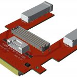
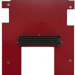
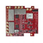
3D Diagrams of PCIe104Z
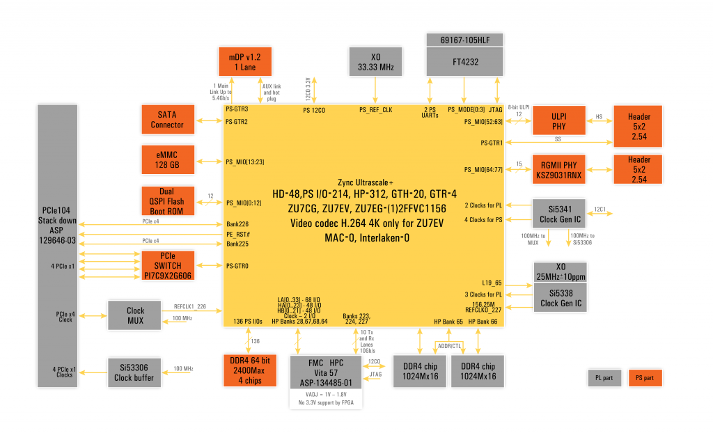
PCIe104Z block diagram
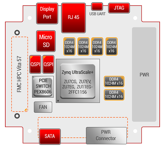
PCIe104Zplacement
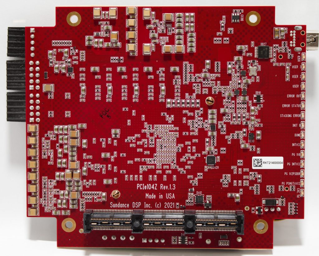
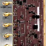
Solder side of PCIe104Z
- PCIe104ZU-7CG-2-E – Dual A53 Core, Speed grade-2 & Extended Temp (MOQ)
- PCIe104Z-ZU7EG-2-E – Quad A53 Core, Speed grade-2 & Extended Temp (MOQ)
- PCIe104Z-ZU7EV-2-E – Quad A53 Core, Speed grade-2 & Extended Temp + H.265 CODEC
- PCIe104Z-ZU11EG-2-E – Quad A53 Core, Speed grade-2 & Extended Temp
All above can also be ordered in -I industrial grade which has a temp of -40 to 100deg C for the Zynq device.