Developing OpenVPX and SOSA-aligned systems often requires significant infrastructure before meaningful software, FPGA, or system-level validation can even begin. Engineers frequently depend on full VPX chassis, backplanes, cooling systems, and power subsystems just to start development and debugging.
At Sundance DSP, we are focused on simplifying that workflow by providing practical development platforms that reduce complexity and accelerate integration. Our growing family of VPX-to-PCIe carrier solutions enables developers to bring VPX payload cards directly into a desktop PCIe environment for rapid prototyping, firmware development, software validation, and system integration. Additional slot profile support is also under development to address the expanding range of OpenVPX and SOSA-aligned architectures used across embedded defense, aerospace, and high-performance computing platforms.
Why VPX-to-PCIe Development Platforms Matter
Traditional OpenVPX development environments can be costly and difficult to scale during early-stage design. By converting a VPX payload module into a standard PCIe-accessible device, developers can immediately begin working from a workstation or development PC without requiring a complete chassis environment.
These carrier boards provide:
- Direct PCIe connectivity to VPX payload modules
- Access to system management interfaces
- FPGA and firmware debug capabilities
- Simplified software bring-up
- Lower development cost and faster iteration cycles
This approach significantly accelerates platform validation while reducing dependency on specialized VPX infrastructure.
Understanding OpenVPX Slot Profiles and Planes
OpenVPX slot profiles, defined in the VITA 65 specification, standardize how high-speed interfaces, control channels, utility signals, and management functions are mapped across the VPX backplane. These profiles ensure interoperability between payload cards, switches, and system infrastructure.
The OpenVPX architecture organizes connectivity into several functional planes:
Data Plane
Typically implemented using Fat Pipes, the Data Plane carries high-bandwidth traffic such as:
- PCIe
- 10/25/40/100Gb Ethernet
- FPGA streaming data paths
Control Plane
Usually implemented using Thin or Ultra-Thin Pipes, the Control Plane handles:
- Low-latency communications
- 1Gb Ethernet management links
- System coordination and control of traffic
Expansion Plane
Provides board-to-board high-speed communication for custom protocols or dedicated interconnects between payload modules.
Management Plane
Implements system management functionality through standards such as:
- VITA 46.11 IPMI/IPMB
- Health monitoring
- Power management
- Intelligent platform management
Understanding these planes is critical when selecting the correct VPX slot profile for a particular payload application.
VPX-to-PCIe Carrier for SLT3-PAY-1F1F2U1TU1T1U1T-14.2.16
The first carrier supports the SLT3-PAY-1F1F2U1TU1T1U1T-14.2.16 slot profile defined within VITA 65 and widely adopted within SOSA-aligned architectures.
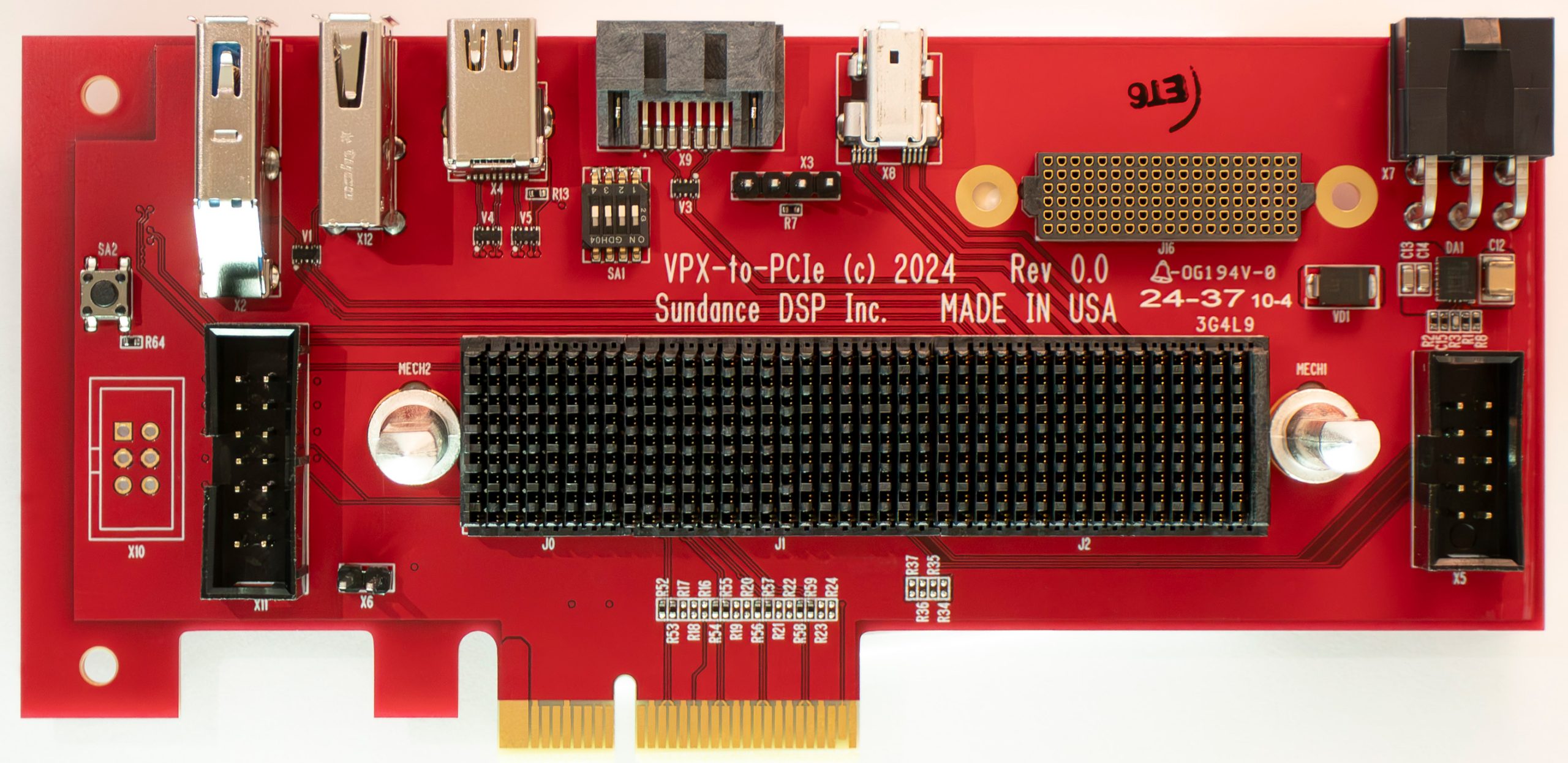
This profile is commonly referred to as the:
SOSA Aligned I/O Intensive Profile
It is designed for payload modules that require extensive external connectivity and balanced high-speed data movement.
Slot Profile Breakdown
1F1F: Dual Fat Pipes
These provide high-bandwidth Data Plane connectivity, commonly used for:
- PCIe
- High-speed Ethernet
- FPGA streaming interfaces
2U: Utility Signals
Provides:
- Power rails
- Timing signals
- Low-speed synchronization
- Platform utilities
1T + 1T: Thin Pipes
Typically associated with the Control Plane and commonly used for:
- 1000Base-KX Ethernet
- Low-latency system communications
- Board management traffic
This carrier enables those Control Plane interfaces to be bridged directly into the host PC environment for software and system-level validation.
1U1T: Mixed Utility and Thin Pipe Connectivity
Adds additional flexibility for custom I/O and management functions.
What the Board Enables
This VPX-to-PCIe platform allows engineers to:
- Operate SOSA payload modules directly from a desktop workstation
- Eliminate the need for a VPX chassis during development
- Access VITA 46.11 management interfaces
- Perform FPGA and firmware debugging through JTAG
- Validate software stacks before system deployment
- Access interfaces including:
- USB
- UART
- SATA
- DisplayPort
- GPIO
- Control Plane Ethernet
The carrier also supports external power input, which is critical because many high-performance VPX payload cards exceed the standard 75W PCIe slot power limitation.
This makes the platform ideal for:
- FPGA development
- Sensor processing payloads
- Data acquisition systems
- High-speed networking applications
- SOSA-aligned I/O-intensive designs
VPX-to-PCIe Carrier for SLT3-PAY-1F1U1S1S1U1U2F1H-14.6.11
The second platform supports the SLT3-PAY-1F1U1S1S1U1U2F1H-14.6.11 slot profile defined within the OpenVPX VITA 65 specification.
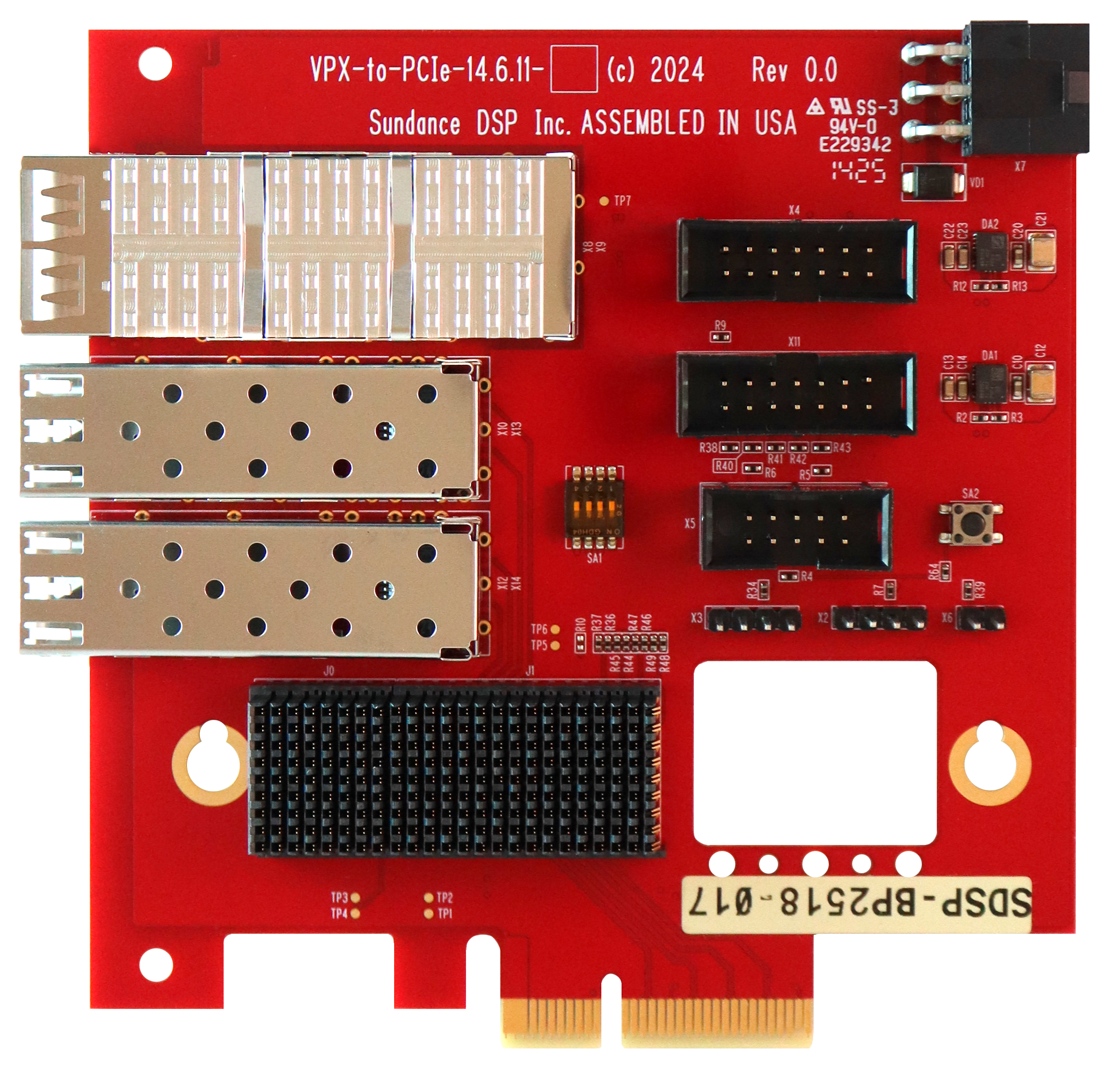
This profile is commonly known as the:
SOSA Aligned Compute Intensive Profile
It is optimized for high-performance compute payloads, including:
- FPGA acceleration modules
- DSP processing cards
- AI inference engines
- High-core-count processor payloads
Slot Profile Breakdown
1F: Fat Pipe
Primary Data Plane connectivity for high-speed communications.
1U: Utility Signals
Provides power and low-speed platform infrastructure.
1S1S: Expansion/Serial Pipes
Supports additional board-level communication interfaces and specialized connectivity paths.
1U1U: Additional Utility Resources
Extends platform management and synchronization capability.
2F: Dual Fat Pipes
Delivers the massive throughput required for:
- FPGA DSP workloads
- AI acceleration
- Multi-stream sensor processing
- High-bandwidth PCIe data movement
1H: Specialized High-Speed Aperture
Within VITA 65 architectures, the “H” designation is commonly associated with specialized apertures or high-speed interface regions used for:
- RF connectivity
- Optical interfaces
- VITA 67.x expansion
- Custom high-speed I/O implementations
What the Board Enables
This carrier platform allows developers to:
- Bring up compute-intensive VPX payloads directly within a PCIe workstation
- Validate FPGA firmware and software before chassis integration
- Access debug and management interfaces
- Test high-throughput PCIe data paths
- Validate Control Plane and Expansion Plane communications
- Interface with external peripherals and instrumentation
Supported interfaces include:
- JTAG
- UART
- USB
- SATA
- DisplayPort
- Ethernet control interfaces
- System management connectivity
The platform is particularly valuable for developers building:
- AI acceleration systems
- Radar processing payloads
- Electronic warfare platforms
- High-speed signal processing modules
- FPGA-based compute engines
Power and Thermal Considerations
One of the biggest engineering challenges when transitioning VPX modules into a desktop development environment is managing both power delivery and thermal performance.
Power Requirements
High-performance VPX payload modules frequently consume significantly more power than a standard PCIe slot can provide.
While a conventional PCIe slot typically delivers:
- 12V
- 3.3V
- Up to 75W total power
Many VPX and SOSA payload modules rely heavily on:
- 12V main payload rails
- Higher current delivery
- Multi-rail power architectures
For this reason, Sundance DSP VPX-to-PCIe carriers include external power connectivity to support demanding FPGA and compute payloads safely and reliably.
Thermal Management
Many VPX modules are designed as:
- Conduction-cooled payloads
- Ruggedized deployable systems
These carriers provide sufficient mechanical clearance and development flexibility for:
- Air-cooled development heat sinks
- Thermal frames
- Bench-top validation setups
This enables engineers to develop and validate modules outside rugged deployment environments while maintaining thermal stability during high-performance operation.
Accelerating SOSA and OpenVPX Development
By combining desktop accessibility with OpenVPX interoperability, Sundance VPX-to-PCIe carriers dramatically simplify the development lifecycle for modern embedded systems.
Key advantages include:
- Faster software and FPGA bring-up
- Reduced infrastructure requirements
- Simplified debugging workflows
- Lower development cost
- Improved validation efficiency
- Support for evolving SOSA-aligned architectures
Whether targeting I/O-intensive payloads or compute-intensive accelerator modules, these platforms provide an efficient bridge between VPX hardware and standard workstation development environments.
As additional slot profiles continue to be introduced, Sundance DSP remains committed to delivering practical development tools that help engineers accelerate deployment and streamline next-generation OpenVPX system integration.