
1. Introduction: The High-Stakes Shift to Secure Edge Computing
For decades, embedded systems engineering treated security as a software-layer afterthought, a firmware patch, a TLS stack, a password policy bolted onto hardware that was never designed to resist a determined physical adversary. That model collapses the moment a system leaves a controlled data center and enters the field: an autonomous ground vehicle exposed to adversarial tampering, a satellite communications payload orbiting beyond any physical guard, a battlefield radio that can be captured and reverse-engineered. In these mission-critical domains, the attacker doesn’t need remote network access; they need only a screwdriver, an oscilloscope, and time with the hardware itself.
This is the terrain of secure edge computing, and it exposes a fundamental engineering tension. Modern autonomous and defense-grade systems demand System-on-Chip (SoC) levels of computational density: multicore processing, real-time deterministic control loops, and reconfigurable logic capable of adapting to evolving sensor and communication standards. Yet that same computational power is worthless if the silicon itself can be cloned, its configuration intercepted at boot, or its cryptographic keys extracted through a power-analysis probe. Reconciling high-speed, flexible computation with hardware-rooted threat mitigation is no longer a niche requirement reserved for defense primes; it is becoming baseline engineering practice for aerospace, medical, industrial, and critical-infrastructure design.
This article examines how Microchip’s PolarFire SoC FPGA family addresses that tension at the silicon level, and how engineering students and embedded developers can gain hands-on experience with this architecture through the Sundance DSP PolarBerry System-on-Module (SoM). We’ll walk through why conventional SRAM-based FPGAs fail modern security requirements, dissect PolarFire’s zero-trust hardware architecture, and provide a practical roadmap for building secure-boot applications using the Microchip Libero SoC Design Suite.
2. Why Conventional FPGAs Fail the Security Test
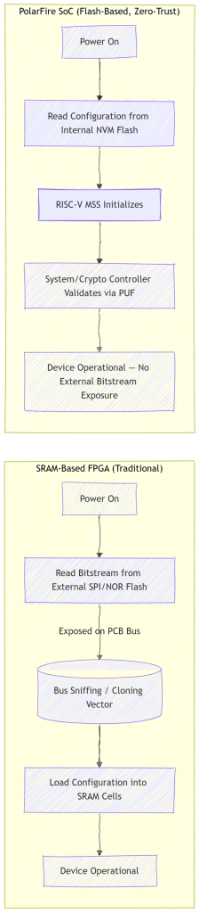
The dominant FPGA architecture for the last thirty years has been SRAM-based reconfigurable logic. SRAM cells are fast to manufacture, dense, and infinitely reprogrammable, but they are volatile. An SRAM FPGA holds no memory of its configuration when power is removed. Every single time the device powers on, its entire logic configuration, the bitstream that defines what the chip actually does, must be streamed in from an external, non-volatile source: typically a discrete SPI NOR flash chip sitting on the same PCB.
This single architectural decision creates a structural security hole that no amount of downstream software hardening can close. During every power-up cycle, the full bitstream traverses an external, physically accessible bus in plaintext or (at best) with encryption that itself depends on external key storage. An attacker with physical access to the board can attach a logic analyzer directly to that SPI bus and capture the bitstream as it loads, a technique that requires no cryptographic breakthrough, only patience and a set of test clips. Once captured, that bitstream can be cloned wholesale onto counterfeit hardware, reverse-engineered to extract proprietary IP, or subtly modified and re-flashed back onto the original device to implant a hardware backdoor before the system boots any of its own security software.
This is the essence of a bus-sniffing and cloning vector: the attack surface exists before the processor has executed a single instruction, which means firmware-level protections, secure boot chains, signed images, and TPM attestation are all downstream of the compromise and cannot prevent it. Bitstream interception and modification attacks specifically target this boot-time window, and they are a documented, practical risk for any system that must survive deployment in a physically unsecured or adversarial environment: an unattended sensor node, a fielded weapons platform, or hardware traveling through an untrusted supply chain.
3. Deep-Dive: The Microchip PolarFire SoC Security Blueprint
On-Chip Non-Volatile Configuration Memory
PolarFire FPGAs invert the SRAM model entirely. The PolarFire family is the fifth generation of Microchip’s non-volatile FPGA devices, built on 28 nm non-volatile process technology, meaning the configuration data is stored permanently inside flash-based logic cells on the die itself. There is no external bitstream load at power-up because nothing is to be loaded externally; the configuration never leaves the silicon. This single architectural choice eliminates the entire class of boot-time bus-sniffing, cloning, and interception attacks that plague SRAM-based competitors, because there is no accessible bus transaction for an attacker to observe or manipulate.
Physically Unclonable Functions (PUF) & Root of Trust
At the heart of PolarFire’s key management is a Physically Unclonable Function. PolarFire and PolarFire SoC FPGAs integrate a lightweight, non-volatile flash-based PUF architecture that exploits subtle process variations in flash memory cells to derive device-unique secrets. Critically, these secrets are derived on-demand during boot or runtime rather than being persistently stored on the device, and the associated helper data used to stabilize the PUF’s output is managed securely without revealing the underlying key. Because the key doesn’t exist in static storage waiting to be read out, there is nothing for an attacker to extract even with full chip decapsulation physically; the key is regenerated fresh from silicon-level entropy each time it’s needed, and the PUF’s behavior itself changes under physical attack, invalidating any attempted key reconstruction.
This PUF forms the device’s Hardware Root of Trust. The secure boot process is anchored in a Hardware Root of Trust that certifies the first instructions executed at power-up are immutable and trustworthy, beginning with an immutable boot ROM while PUF-protected secure non-volatile memory (sNVM) secures keys and proprietary loaders. In practice, the system controller extracts two distinct PUF master secret keys from the device: one used for wrapping design security keys, and a second dedicated to sNVM encryption and authentication.
The TeraFire Crypto Accelerator & DPA Defense
Key derivation is only half the equation; those keys must be used without leaking information through side channels. PolarFire SoC devices offload cryptographic operations to a hardened crypto co-processor (Athena F5200B) that handles RSA, ECC, AES, SHA, and HMAC operations, offloading crypto functionality for DPA resistance and CAVP-certified algorithm compliance, paired with an integrated true random number generator for secure cryptographic operations. This co-processor is complemented by side-channel attack resistance built on Rambus’ Differential Power Analysis (DPA) countermeasure portfolio from Cryptography Research, and PUF-protected key storage ensures derived keys are never exposed externally. Because the crypto engine is hardened silicon rather than a software routine executing on a general-purpose core, the power-consumption signature of each operation is deliberately flattened, denying an attacker the statistical leverage needed for differential power analysis.
Active Anti-Tamper & Zeroization
Beyond boot-time protection, PolarFire SoC devices maintain continuous environmental monitoring throughout operation. The system controller watches for out-of-spec voltage, temperature, and clock conditions; the classic toolkit of a fault-injection attacker attempting to induce glitches that bypass authentication checks or corrupt secure logic. When a tamper event is detected during the secure boot sequence specifically, a BOOT_FAIL tamper flag is raised in the FPGA fabric’s tamper macro, and subsequent firmware payloads are blocked from loading and executing, with the designer free to define how that flag is handled downstream in their fabric design. This tamper-response architecture extends the device’s design security posture to include anti-cloning protection, bitstream protection, key management, FPGA hardware access control, and physical memory protection as coordinated, silicon-level responses to a breach attempt.
Single Event Upset (SEU) Resilience
The same non-volatile flash-cell architecture that defeats bus-sniffing also delivers a second, unrelated benefit critical to aerospace and defense applications: immunity to Single Event Upsets. SRAM-based FPGA configuration memory is a lattice of bistable latches, and a single energetic neutron or heavy ion strike, the kind of radiation routinely encountered at altitude or in orbit, can flip one of those latches, silently corrupting the device’s logic configuration without any power cycle to trigger a reload. PolarFire’s flash-based configuration cells store their state as trapped charge in a floating gate rather than as a powered bistable circuit, making the configuration itself structurally immune to this class of radiation-induced upset. That reliability property is precisely why PolarFire-class devices see disproportionate adoption in satellite payloads, avionics, implantable and diagnostic medical electronics, and other domains where an undetected single-bit configuration flip is not merely a bug but a mission-ending failure.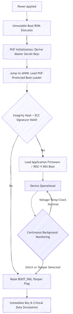
4. The Sandbox: Learning with the Sundance DSP PolarBerry SoM
Understanding PolarFire’s security architecture in the abstract is one thing; wiring up a high-speed board with proper power sequencing, SERDES routing, and clock distribution just to get a development platform running is another challenge entirely, and one that has historically kept students away from hands-on FPGA security work. The Sundance DSP PolarBerry System-on-Module makes it easy to develop for and integrate Microchip’s PolarFire SoC, pairing a low-power FPGA with a secure, four-application-core, 64-bit Linux-capable RISC-V subsystem, without requiring the learner to design that high-speed layout themselves.
Form factor and interfaces. The PolarBerry SoM measures just 55mm by 85mm and operates across a 0°C to +70°C temperature range, and it can function either as a standalone single-board computer or as a module on a carrier board. It carries a Microsemi PolarFire FPGA (MPFS250T-FCVG484) built around a penta-core processor arrangement, one RV64IMAC monitor core plus four RV64GC application cores, combined with FPGA fabric offering roughly 254,000 logic elements, 784 math blocks, and 16 SERDES lanes running up to 12.5 Gbps. Connectivity includes a 100/1000Base-T Ethernet port, two CAN 2.0 interfaces, a JTAG programming interface, and 4GB of onboard eMMC storage, alongside a 40-pin Raspberry Pi-compatible header providing up to 26 GPIOs for rapid peripheral prototyping, a deliberate design choice that lets learners bring existing Raspberry Pi HAT experience directly into FPGA/RISC-V development.
RISC-V and FPGA fabric interaction. The deterministic, coherent RISC-V cluster and the programmable logic fabric on PolarBerry are not separate chips awkwardly bridged together; they share the same PolarFire SoC die and memory subsystem. The RISC-V CPU implementation uses a simple five-stage, single-issue, in-order pipeline that avoids the Meltdown and Spectre vulnerability classes found in common out-of-order processors, and all five cores are coherent with the memory subsystem, allowing a learner to mix deterministic, real-time control tasks running on dedicated application cores with a full Linux environment running concurrently on others, while offloading latency-critical signal processing or cryptographic acceleration into custom fabric logic sitting right next to the CPU cluster.
A theoretical secure-boot walkthrough with Libero SoC. Building a sample secure-boot application on PolarBerry follows a conceptual sequence within Microchip’s Libero SoC Design Suite. A learner begins by defining the RISC-V MSS configuration, enabling the specific application cores and memory-mapped peripherals the project requires, then partitions a region of the device’s sNVM for storage of a custom boot loader, as described in PolarFire SoC’s boot mode 2 flow. In this mode, the system controller loads the boot loader onto the monitor core’s dedicated tightly-coupled memory and checks the integrity and authenticates the contents of sNVM before handing off execution. Within Libero, the designer generates the security policy, selecting which PUF-derived key wraps the sNVM contents, synthesizes the fabric design containing any custom logic, and then uses the associated programming tools to provision the device via JTAG. If integrity or signature verification ever fails during this sequence, the fabric’s tamper macro raises the BOOT_FAIL flag, which the learner’s own fabric logic can be designed to observe and act upon, giving a direct, hands-on view of the same zeroization pathway used in fielded defense systems.
5. Practical Learning Strategies & Conclusion
For a student approaching this stack for the first time, a staged roadmap works best. Start by getting comfortable with Libero SoC’s project and constraint-management workflow using simple fabric designs, blinking GPIOs, and basic UART communication before touching any security features at all. Next, bring up the RISC-V MSS configuration and get a minimal Linux or bare-metal application booting through the standard (non-custom) boot path, so the baseline hardware flow is well understood. Only then move into sNVM provisioning and PUF-backed key wrapping, deliberately triggering and observing a BOOT_FAIL condition in a lab setting to see the tamper-response chain in action. Finally, layer in the crypto co-processor APIs for signing and encryption, and study how DPA countermeasures are configured within the toolchain rather than treating them as an invisible black box.
The demand for engineers fluent in this discipline, where digital logic design, applied cryptography, and physical security converge on a single die, is accelerating well beyond the defense and aerospace sectors that first drove it, extending into medical devices, industrial control systems, and any infrastructure that can no longer assume physical access implies trust. Platforms like PolarFire SoC, made approachable through accessible hardware like the PolarBerry SoM, are turning what was once a specialized, classified-adjacent skill set into a learnable engineering discipline, and the engineers who master it early will be the ones architecting the trustworthy edge of the next decade.