
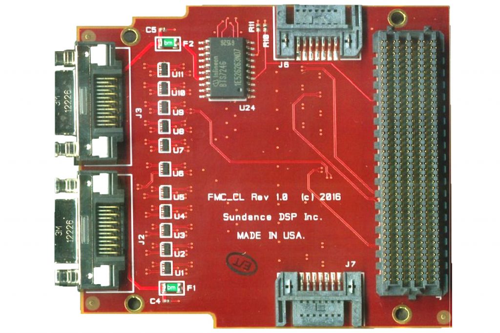
FMC-GPIO module: the split-architecture design ships as an FMC module, a matching auxiliary card, and two flex cables. Full product page and STEP files.
The Hook: Why Your FMC Breakout Board Is Fighting You
Every FPGA engineer who has built a hardware-in-the-loop (HIL) rig, a signal-communications testbed, or a rapid-prototyping bench has run into the same wall: the FMC connector gives you dense, high-quality I/O, and then the mechanics of the platform make that I/O almost unreachable.
The Mechanical Trap
An FMC site sits deep inside a 2U server, a PXIe controller slot, or a ruggedized enclosure. The moment you need to probe a differential pair, sync an external trigger, or route a control line to a device under test, you’re threading cable bundles through a chassis that was never designed to expose them. The usual fix, a flying-lead breakout board bolted to the FMC connector, turns into a rat’s nest of loose wires draped across a card cage, one accidental tug away from a bent pin or a dropped connection during a 72-hour soak test.
Fixed-Voltage Friction
Many breakout solutions solve the mechanical problem by adding onboard level-shifter ICs, locking the board to a small set of supported I/O standards. That’s a reasonable trade-off until your test plan changes, say, from 1.8V HSTL to 2.5V LVDS, and now you’re either re-spinning a board or accepting the propagation delay and skew that level-shifting devices inevitably add. On a timing-sensitive interface, that’s not a rounding error; it’s a variable you now have to characterize and subtract out of every measurement.
Carrier Mismatch
LPC and HPC carrier boards are electrically and mechanically different animals. A breakout board built for one doesn’t sit right or connect at all on the other. Teams that iterate across multiple carrier platforms (which is most teams doing serious FPGA prototyping) end up maintaining two, sometimes three, parallel sets of breakout hardware just to keep pace with whichever carrier is on the bench that week.
Single-Purpose FMC Waste
An FMC site is a precious resource, often the only expansion path a carrier board offers. Dedicating that slot to pure GPIO breakout means giving up the option to simultaneously bring up a high-speed storage interface. On a data-logging or telemetry-capture design, that’s a real architectural cost: you either accept a second FMC site you don’t have, or you accept that your GPIO board is doing nothing but GPIO.
The Solution: Inside the Sundance DSP FMC-GPIO Architecture
The FMC-GPIO is built around a straightforward premise: don’t fight the chassis, route around it, and don’t compromise the signal to do it.
Split-Architecture with Auxiliary Card
The module ships as two physical boards connected by a flex cable, not one. Of the four 26-pin SDR connectors, two live directly on the FMC module itself. The remaining two are relocated onto a dedicated auxiliary card, linked back to the FMC module through rugged flex cables (Molex 152660343). That auxiliary card is designed to mount into a PC, PXIe, or other chassis back panel, bringing those connectors out to the rear of the enclosure.
The effect is structural, not cosmetic: half your I/O interface moves from “buried inside the card cage” to “accessible from the back panel,” with a fixed, mechanically secured cable run replacing improvised wiring. You get a stable, repeatable connection point for test equipment, probes, or a device under test, without opening the chassis every time you need to touch a signal.
Mechanical layout: the FMC-GPIO module stays seated on the FMC site inside the chassis, while the auxiliary card carrying SDR3/SDR4 mounts to the rear bracket, connected by a fixed flex-cable run instead of loose cabling.
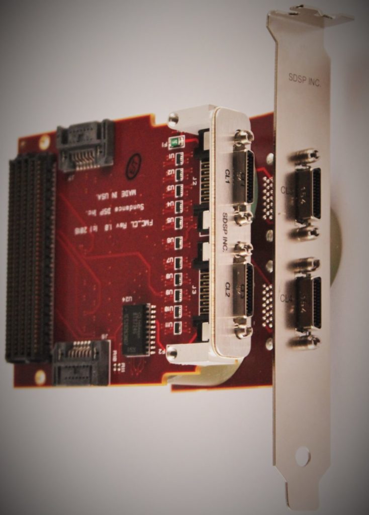
Auxiliary card attached to the FMC module by the two Molex 152660343 flex cables, ready for back-panel mounting.
44 Differential I/O Pairs Across LA and HA Banks
The four SDR connectors map cleanly onto the FMC pin banks and scale with carrier capability:
- SDR1 — 11 differential pairs on the LA bank (1 clock-capable), accessible on LPC FMC
- SDR2 — 11 differential pairs on the LA bank (2 clock-capable), accessible on LPC FMC
- SDR3 — 11 differential pairs, 10 on the HA bank plus 1 clock-capable pair on LA, accessible on HPC FMC
- SDR4 — 11 differential pairs on the HA bank (3 clock-capable), accessible on HPC FMC
Quick reference:
| Connector | Bank | Diff. Pairs | Clock-Capable | FMC Site Required |
|---|---|---|---|---|
| SDR1 | LA | 11 | 1 | LPC |
| SDR2 | LA | 11 | 2 | LPC |
| SDR3 | LA + HA | 11 (10 HA + 1 LA) | 1 | HPC |
| SDR4 | HA | 11 | 3 | HPC |
| Total | — | 44 | 7 | — |
That’s 44 differential I/O pairs total, split so that SDR1/SDR2 alone give you full functionality on an LPC site, while SDR3/SDR4 activate only when the module is seated on an HPC site. Drop the FMC-GPIO onto an LPC carrier, and you get two working SDR connectors and full LA-bank access; drop the same board onto an HPC carrier and all four connectors, including the HA bank, come alive. One part number, no re-spin, no separate SKU for LPC versus HPC; the board simply exposes what the connector underneath it supports.
Pure Passthrough Design: No Hardwired Level Shifters
This is the architectural decision that matters most for signal integrity. The FMC-GPIO carries no onboard level-shifting devices in the signal path. It is, by design, a pass-through unit: I/O voltage is set by the FPGA carrier’s VADJ rail, not by a fixed component on the breakout board itself.
Practically, that means the I/O standard your FPGA fabric is configured to drive, whatever LVDS, HSTL, or other standard your VADJ setting establishes, is what actually appears at the connector, natively, with no intermediate translation stage. There’s no shifter propagation delay to characterize, no additional skew source to budget for in your timing closure, and no voltage ceiling imposed by the breakout hardware. Change your VADJ setting to move between voltage standards, and the FMC-GPIO simply carries whatever you send it. The board adapts to your interface requirements instead of constraining them.
Hybrid Data Routing: Dual SATA on the Same Slot
Alongside the GPIO banks, the FMC-GPIO carries one multi-gigabit transceiver on the LA bank and one on the HA bank, each of which can be configured as an optional SATA interface for direct-to-disk connectivity. This is not automatic: it requires an appropriate FPGA transceiver IP core (SATA controller logic mapped to the carrier’s GTP/GTX/GTH-class resources, depending on device family) and correct pinout configuration in your design. On an LPC carrier, that gives you a single SATA channel alongside your GPIO; on an HPC carrier, both transceivers are available, giving you dual SATA in addition to the full 44-pair I/O set. Supported SATA generation and achievable throughput will follow from your specific carrier’s transceiver capability and IP selection; confirm against your carrier’s datasheet before committing to a data-rate target.
That combination, general-purpose differential I/O plus optional high-speed disk interfaces, means a single FMC-GPIO board and a single FMC slot can support both a control/instrumentation function and a direct-to-disk data path in the same design. You’re not choosing between GPIO breakout and storage bring-up; the same slot, and the same board, can be architected to do both.
Practical Considerations Before You Design It In
A pass-through architecture is a strength, but it comes with responsibilities which I should flag:
- VADJ discipline is on you. Because the FMC-GPIO applies no independent voltage regulation or protection in the signal path, the I/O standard and voltage level at every SDR pin is exactly whatever your FPGA carrier’s VADJ rail is set to. There’s no onboard safety net if VADJ is misconfigured; get your carrier’s I/O bank voltage planning right before you connect a device under test.
- The auxiliary card needs a physical mounting point. Routing SDR3/SDR4 to the back panel is a mechanical win, but it does assume your chassis has (or can accommodate) an open bracket slot, a PC expansion slot, or a PXIe module slot, for the auxiliary card. It’s not a zero-modification, drop-in fix for every enclosure.
- Flex cable routing is still a mechanical design step. The Molex 152660343 flex cables replace loose flying leads with a fixed, connectorized run, which is a meaningful improvement for long-duration soak or vibration testing, but you’ll still want to plan the routing path and strain relief inside your chassis during layout, rather than treating it as an afterthought.
- Compare against Sundance’s other GPIO options if your application calls for fixed-voltage translation. The FMC-GPIO’s sibling product, the FMC-GPIO68SE, takes the opposite approach, auto-sensing level-translator ICs supporting 1.8V–5V single-ended I/O with an optional pass-through build option. If your use case genuinely needs onboard level translation rather than native VADJ pass-through, that’s the board to evaluate instead.
None of this changes the core value proposition; it’s context a design review should have on hand before the board goes on the BOM.
Ideal Use Cases
Hardware-in-the-Loop testing in defense and signal communications: Where deterministic, low-skew signal access to a device under test matters, and where an unreachable, buried FMC connector isn’t an option for a rig that needs to be re-cabled repeatedly over the life of a test campaign. Applicable across Xilinx/AMD, Intel/Altera, and Microchip PolarFire carrier ecosystems, since the FMC-GPIO’s behavior is governed by the VITA 57.1 LPC/HPC connector definition, not by a specific FPGA vendor’s I/O bank implementation.
Rapid prototyping across shifting LPC/HPC carrier boards: Teams evaluating multiple FPGA carrier platforms (Xilinx/AMD, Intel/Altera, Microchip PolarFire) can standardize on one GPIO breakout board and let it automatically scale its capability to whichever site it’s populated on.
Low-overhead direct-to-disk telemetry streaming: Applications that need to capture high-bandwidth data to local storage without dedicating a separate FMC site or PCIe endpoint purely to a storage controller.
Conclusion: A Low-Cost Insurance Policy for the Lab
The FMC-GPIO doesn’t try to be clever about signal conditioning; it deliberately avoids getting in the way of the signal at all. By moving half the I/O density out to a chassis back panel, staying voltage-agnostic through a true pass-through design, and folding in optional dual-SATA capability on the same board, it addresses the mechanical, electrical, and architectural friction points that turn a simple breakout task into a recurring engineering cost.
For teams that iterate across carrier platforms, run long-duration HIL campaigns, or need storage and GPIO out of the same slot, it’s a low-cost way to stop re-solving the same breakout problem on every new build.