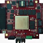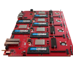

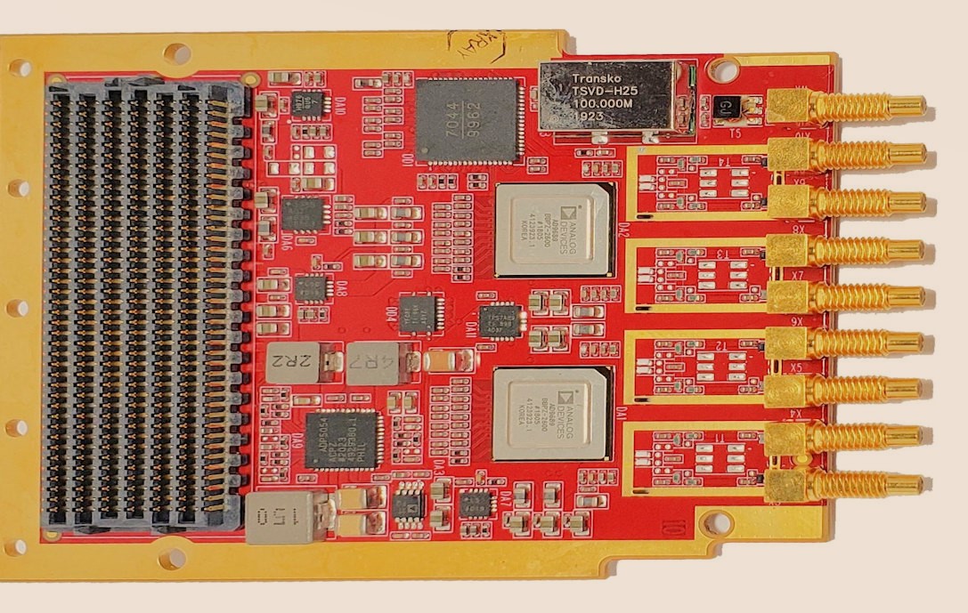
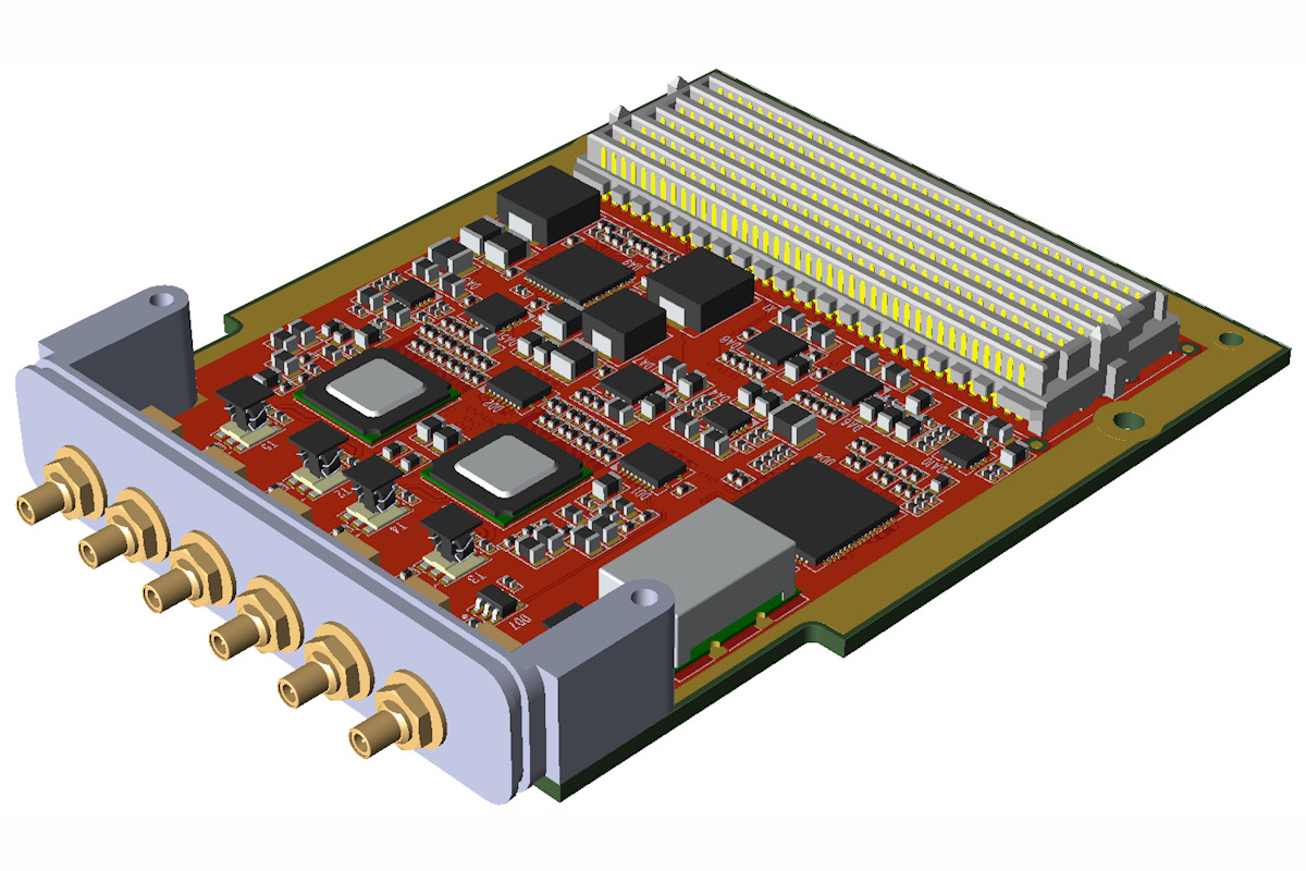
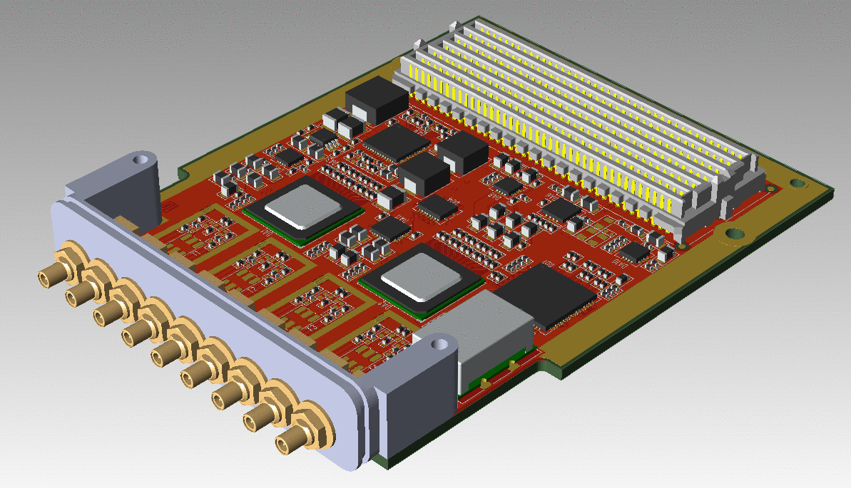
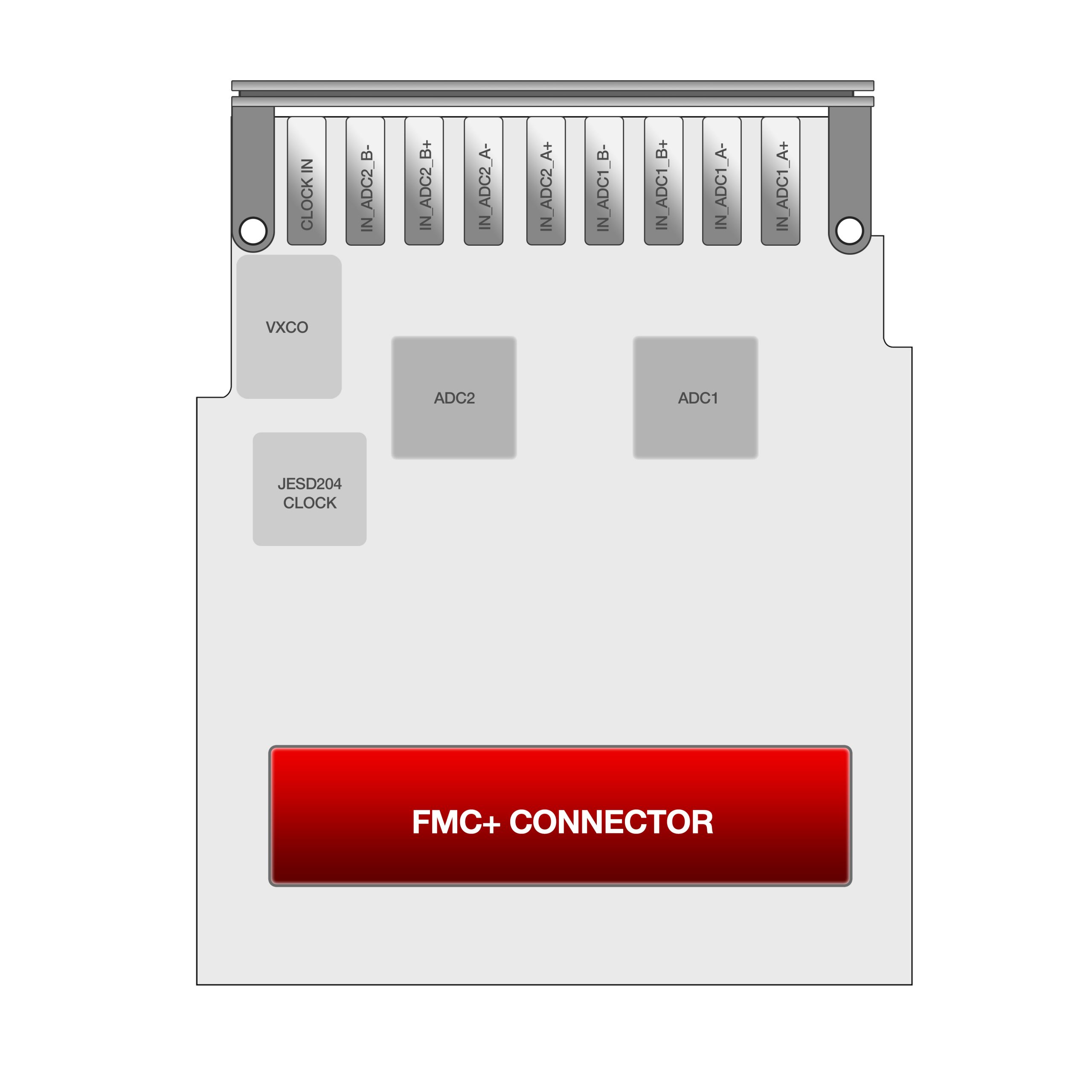
FMCP-ADC3P0 ADC FMC+ (or FMC as build option) comes as an AC coupled differential (or single-ended, as a build option) FMC+ ADC module, without any balun on the differential input path to provide maximum accuracy. It supplies four channels (quad channels) of ADC with 3GS/s each at 14bits by using 2 AD9208 ADC ICs (or AD9689BBPZ-2600 for 2.6GS/s, or 2000GS/s) . ADC input is to interface with the JESD204B IP core. The full power bandwidth of this module is 5GHz. Trigger and external clock input connectors are available on the module. The trigger input allows the user to add a timestamp to the sample stream from ADC. This ADC can come with FMC or FMC+ connector. If FMC connector is used then it will only have 2 channels.
In this module, the ADC input is connected directly to the input differential signal, and the maximum input swing is 1.7V and 2.7V for the differential and single-ended, respectively.
Board clocking structure has been designed based on HMC7044, which provides the possibility of deterministic latency and subclass one synchronization between multiple ADCs.
The module uses 2 ADCs. This device is a JESD204B complaint. They can work at various sample rates, and there is a possibility to enable decimation for the ADC.
Board provides internal VCXO and TCXO clocks. In this case, clocks from HMC7044 go to ADC. This IC also provides the SYSREF clock with known and adjustable delays. According to JESD204B, this also provides REF CLK and SYSREF CLK for FPGA, to achieve the requirement of subclass 1 JESD204B.
The FPGA REF CLK can be used to clock the Rx path. Inside the FPGA transceivers, there are two PLLs. One QPLL – is shared for four transceivers (called quad)- and CPLL one for each transceiver.
Features
- FMC+, Vita 57.4 compliant, form factor, HPC (optionally can have FMC interface with only two ADC channels)
- Conduction cooled
- 4 channels of ADC at 3GS/as 14 bits, using 2 AD9208 ICs (or AD9689BBPZ-2600 for 2.6GS/s)
- flexible clocking
- trigger and external clock inputs
- supported by JESD204C class 1 supported by using HMC7044 clock IC
ADC parameters from ADI datasheet:
- 14-Bit Resolution, Dual-Chanel, 3000MSPS ADC;
- -3 dB bandwidth – 9GHz;
- Full power bandwidth – 5GHz;
- INL: ±6 LSB (Ta = 25);
- DNL: ±0.4 LSB (Ta = 25);
- NF: 24.5 dB;
- Spectral Performance (fIN = 255 MHz at –2 dBFS):
- SNR: 60.2 dBFS
- NSD: –152 dBFS/Hz
- SFDR: 71 dBFS
- ENOB: 9.6 Bits
- Spectral Performance (fIN = 3950 MHz at –2 dBFS):
- SNR: 55.1 dBFS
- SFDR: 58 dBFS
- ENOB: 8.5 Bits
- Input Full-Scale differential: from 1.13 to 2.04 VPP(software selectable). 1.7V default.
Board Parameters:
Signal inputs:
- Input type: Differential (single-ended – option), AC coupled
- Input impedance: 200 Ohm(differential)
- Maximum input voltage range for AC coupled input: 2 Vpp (differential).
Trigger input :
- Input type: DC – coupled, single-ended, 3.3V logic, ESD protected;
- Input impedance : >100 kOhm;
- Frequency range: DC – 10 MHz;
- Maximum input voltage – 6V;
- Logic “0” voltage <0.8V;
- Triggering voltage >2V.
Estimated total Board Power Dissipation: 20W max.
Applications
- Defense and Aerospace
- Diversity multiband, multimode digital receivers
- 3G/4G, TD-SCDMA, W-CDMA, GSM, LTE, LTE-A
- Electronic test and measurement systems
- Phased array radar and electronic warfare
- DOCSIS 3.0 CMTS upstream receive paths
- HFC digital reverse path receivers
 |
 |
 |
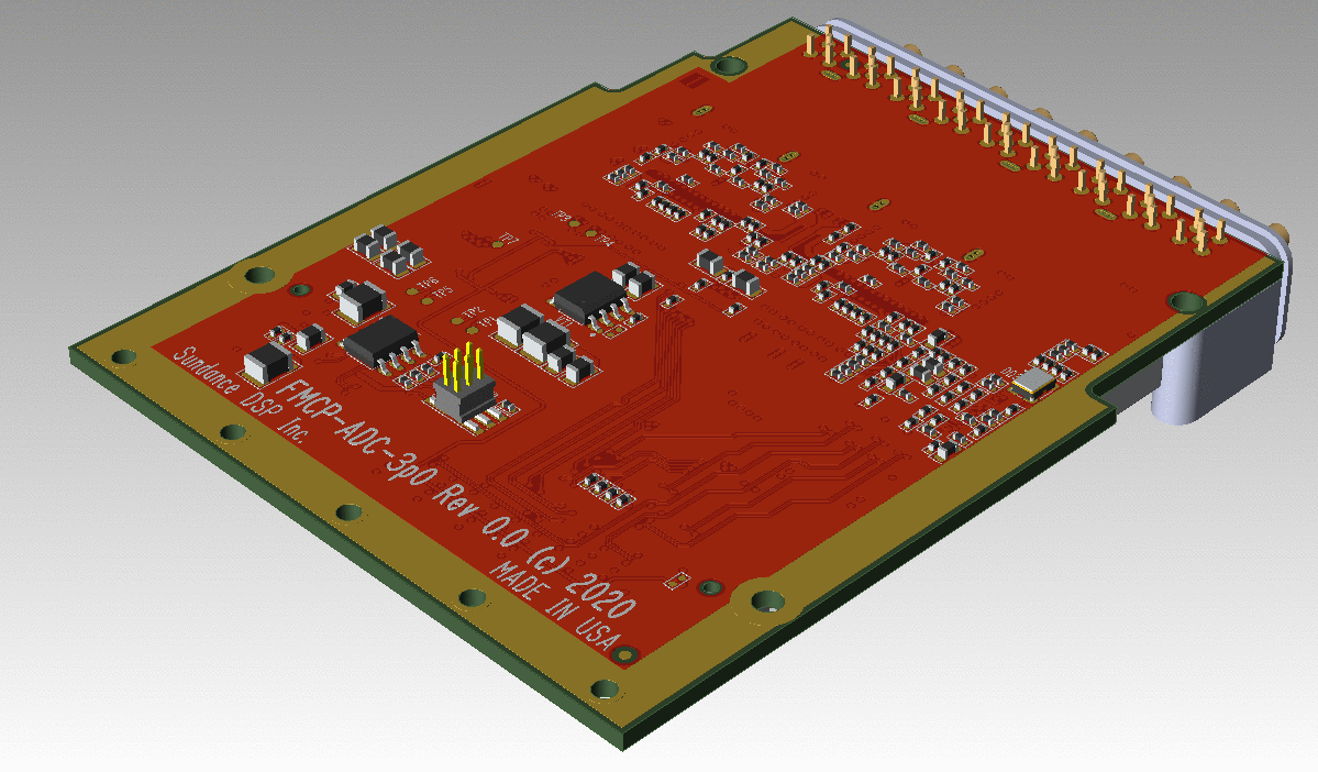 |
| component side differntial input | component side for single ended input | component side for differential input | solder side for differntialinput |
 Placement Diagram
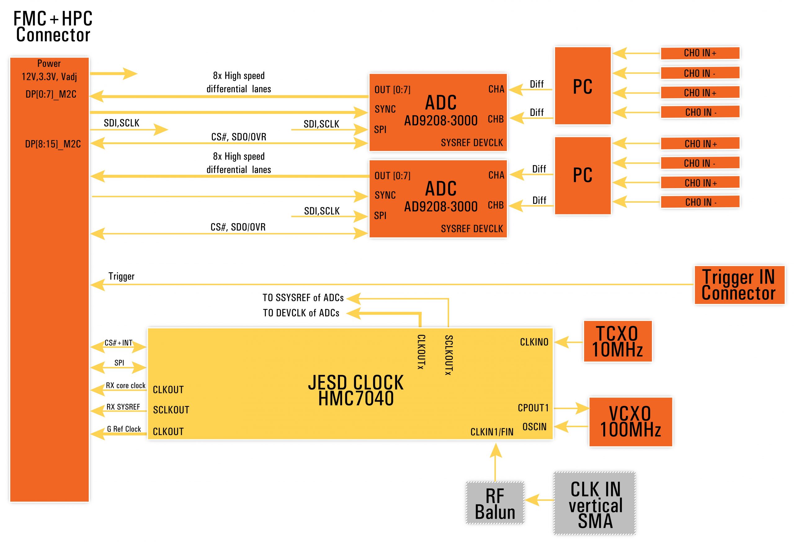
Block Diagram
A complete Vivado project showing the capture of ADC signals by using the Xilinx JESD204B IP core with sample data sent to host via carrier card PCIe interface.
This built in USA module can optionally come with an FMC rather than an FMC+ connector in which case only 2 channels will be available. The default FMC+ comes with 4 ADC channels. There are a many ordering options so please study them carefully and select the one suitable for your application:
This module can be populated as FMC with 2 channels or FMC+ with 4 channels. Below options are available.
| Full Mezzanine Board Name | Number of ADCs installed | ADC Type | Sample Rate | FMC/FMC+ |
| FMC-ADC2p0 | only DA1 | AD9689BBPZ-2000 | 2.0 GSPS | FMC |
| FMC-ADC2p6 | only DA1 | AD9689BBPZ-2600 | 2.6 GSPS | FMC |
| FMC-ADC3p0 | only DA1 | AD9208 | 3.0 GSPS | FMC |
| FMCP-ADC2p0 | Both DA1 and DA2 | AD9689BBPZ-2000 | 2.0 GSPS | FMC+ |
| FMCP-ADC2p6 | Both DA1 and DA2 | AD9689BBPZ-2600 | 2.6 GSPS | FMC+ |
| FMCP-ADC3p0 | Both DA1 and DA2 | AD9208 | 3.0 GSPS | FMC+ |
FMCx-ADCyyy–z-w
x can be P for FMC+, or blank for FMC
yyy can be 3p0 for 3GS/s sampling, 2p6 for 2.6GS/s sampling per channel and 2p0 for 2GS/s sampling
z can be blank for single ended, or d for differential
w blank means extended temperature and I indicate industrial grade
Example orders:
FMCP-ADC2.6-s FMC+, 4 ADC channels each of 2.6GHz sampling, Single ended
FMC-ADC2p0-d FMC module with 2 channels of ADC at 2GHz sampling rate, differential signals
Default module is FMCP-ADC2p0 FMC+ with 4 single ended ADC channels at 2.0GS/s , extended temperature