
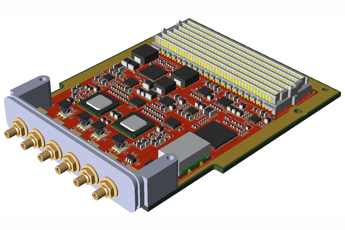
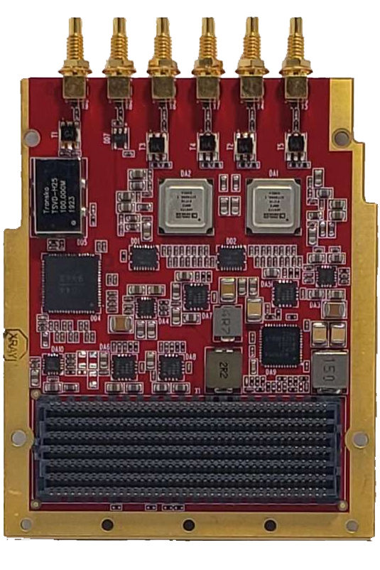
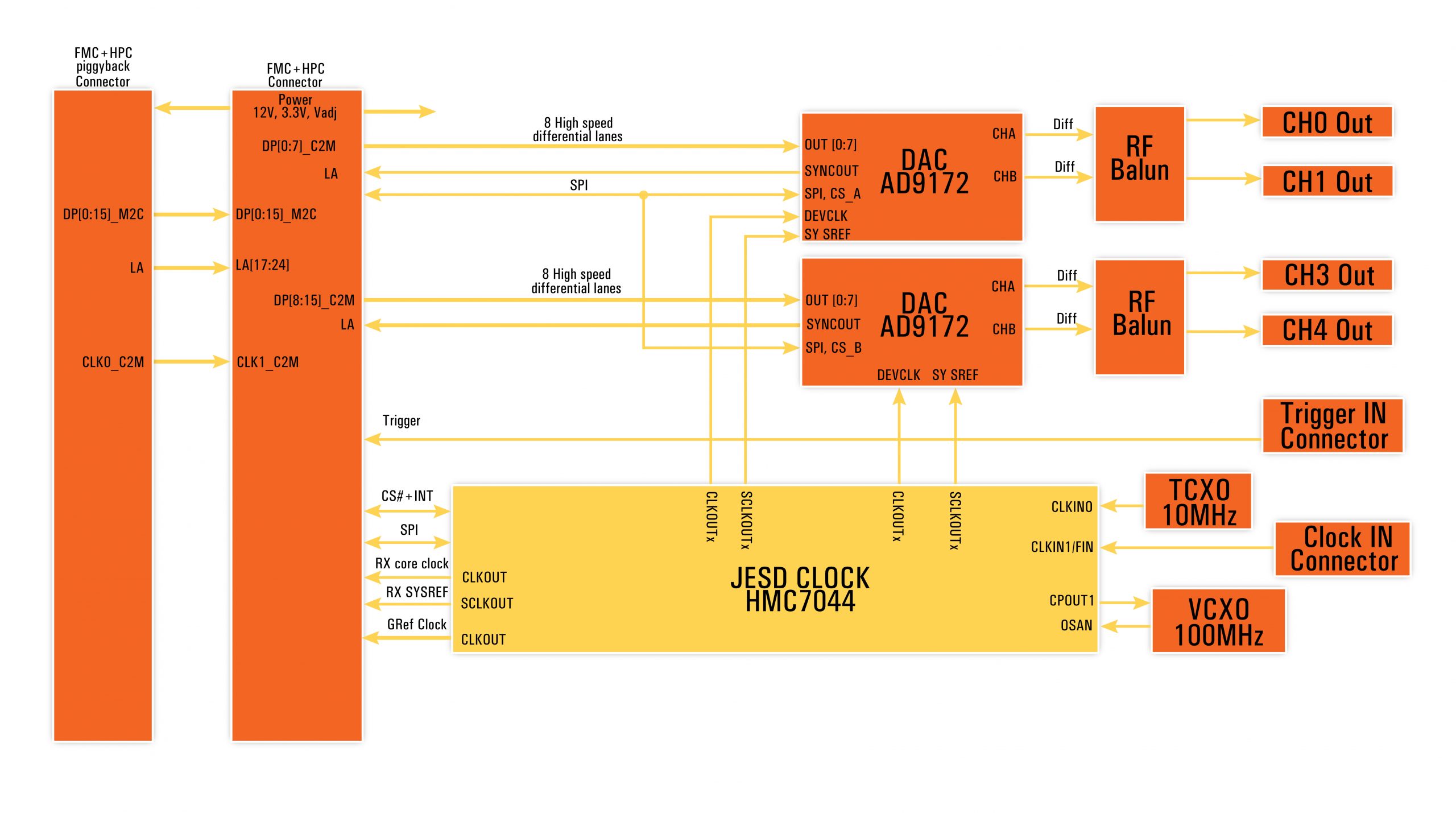
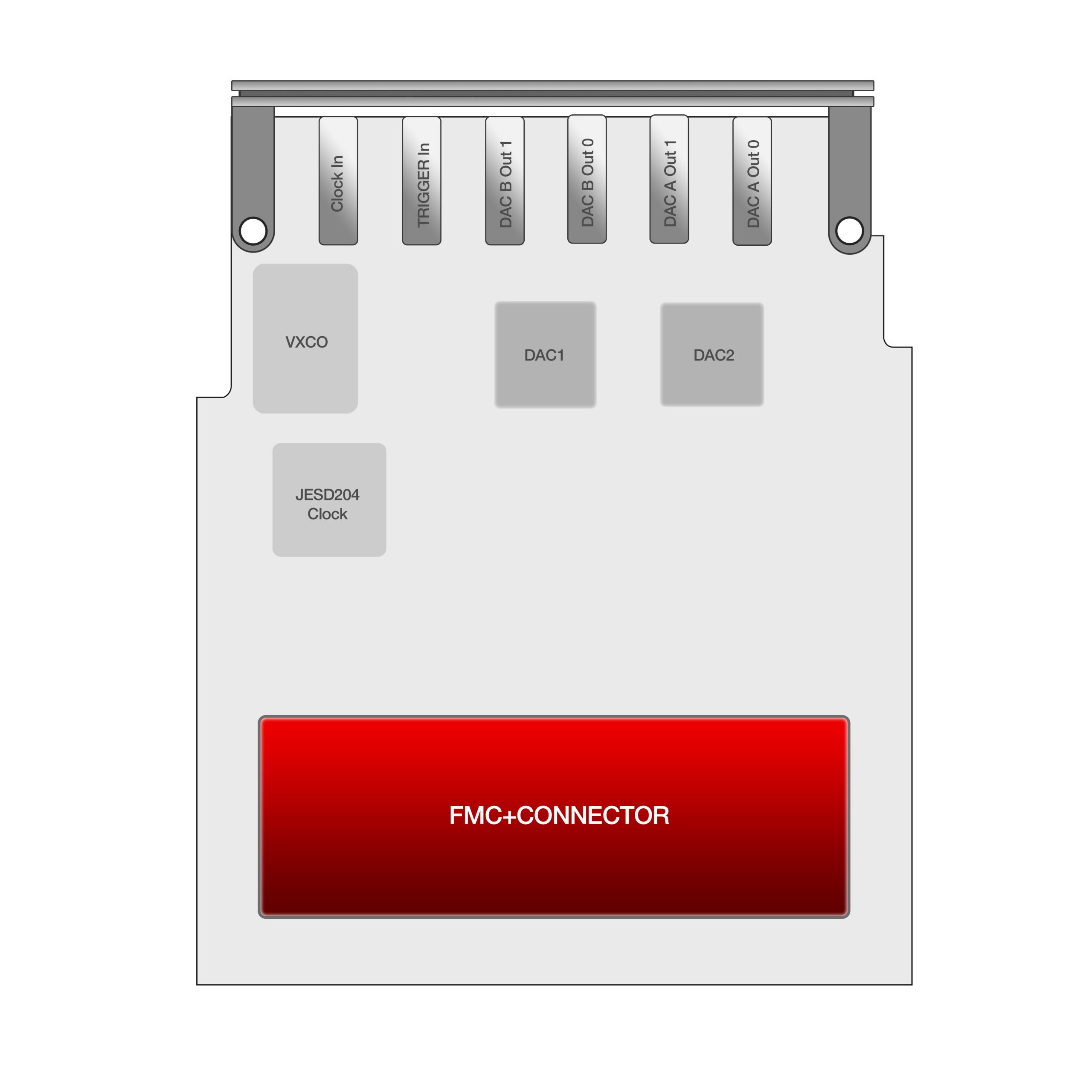
FMCP-DAC12p0 is a four channels DAC module based on the industry-standard FMC+ standard. It utilizes two onboard AD9172 for Digital to Analog Conversion, and interfaces work through the JESD204B IP core. This module is an advanced High-speed Digital to Analog converter in the market with a 16-bit resolution capable of a sample rate at 12.6 GSPS and has dual channels in a single package. Each DAC IC can be configured via the SPI interface separately.
The module includes an HMC7044 – High-performance 3.2GHz JESD204B jitter attenuator for obtaining the best results. Onboard the module is a 100 MHz onboard VCXO; and 10 MHz TCXO as reference clock, or external user reference clock;
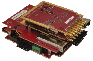
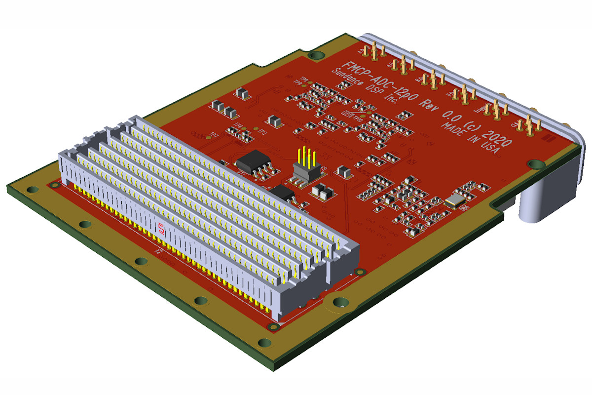
To maximize utilization of FPGA carrier card transceivers, FMCP-DAC12p0 has a carrier-type FMC+ connector on the solder side. So an FMCP-ADC3p0 can be piggy-backed by this module which means, all 16 Rx and TX transceivers of carrier cards can be used. This feature is the optimization of transceivers’ use offered by this module. On one FMC+ site, a four-channel DAC and a four-channel ADC can coexist and provide substantial savings in space and resource use. Image below show the combination PCIe104Z+ and the FMC+ interposer module with the FMCP-DAC12p0 and ADC3p0.
Features
- Two AD9172 dual 16-bit 12GSPS Digital to Analog Converter, JESD204B based.
- HMC7044 – High performance 3.2GHz JESD204B jitter attenuator.
- Six connectors, SSMC type:
- Four connectors for DAC output signals
- One for reference clock
- One Trigger input
- JESD204B Subclass 1 capable;
- 100 MHz onboard VCXO;
- 10 MHz onboard TCXO as reference clock, or external user reference clock;
- Vadj supported voltages:1.8V, 2.5V, 3.3V;
- FMC+ connectors:
- First connector – HPC FMC+ mezzanine connector (ASP-184330-01) will use LA banks for digital interface, 16 Ten-gigabit pairs will be used to transmit data from a carrier to DACs.
- Second connector – HPC FMC+ carrier connector (ASP-184329-01) provide piggyback connectivity of FMCP_ADC3p0 board.
- Trigger input: Trigger input allows users to synchronize various applications, or to start DAC output when the trigger is fired.
- Input type: DC – coupled, single-ended, 3.3V logic, ESD protected;
- Input impedance : >100 kOhm;
- Frequency range: DC – 10 MHz;
- Maximum input voltage – 3.3V;
- Logic “0” voltage <0.4V;
- Triggering voltage >1V.
Applications
- Defense and Aerospace
- Diversity multiband, multimode digital receivers
- 3G/4G, TD-SCDMA, W-CDMA, GSM, LTE, LTE-A
- Electronic test and measurement systems
- Phased array radar and electronic warfare
- DOCSIS 3.0 CMTS upstream receive paths
- HFC digital reverse path receivers
 |
 |
 |
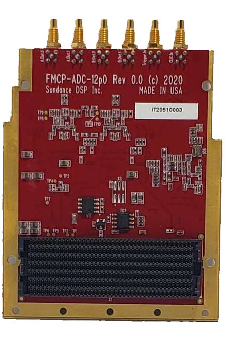 |
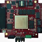
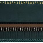
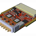
| rendered image component side | rendered image solder side | component side | FMCP-DAC12p0 solder side showing piggy back FMC+ connector |
A complete Vivado project showing sample digital signals sent to DAC ICs by using the Xilinx JESD204B IP core is provided.
FMCP-DAC12p0