
Introduction
In rugged embedded computing, it’s tempting to treat every new form factor as a replacement for the last one. VNX+ is often described that way, as “the next VPX” or “VPX, but smaller.” That framing misses the point. VPX (ANSI/VITA 46/48/65) and VNX+ (ANSI/VITA 90) were never meant to compete for the same slot in the same system. They were designed to solve two different halves of the same SWaP (Size, Weight, and Power) problem, and, critically, to interoperate. A system architect can put both standards in the same chassis, on the same backplane, in the same program, without redesigning either one around the other.
This article looks at why that’s true: the size and power envelopes that define each standard, the markets each one targets, and the mechanical reality that makes it possible to drop a VNX+ module directly into a VPX chassis using a passive adapter, a product SundanceDSP offers today, the VNX+ to 3U VPX Adapter.
VPX: The Established Backbone of Rugged Modular Computing
VPX traces back to VITA 46, ratified in the mid-2000s as a response to VME64x running out of headroom for high-speed serial fabrics. VITA 65 (OpenVPX) followed to standardize the profiles, slot roles, and backplane topologies that make VPX modules from different vendors interoperable rather than just mechanically similar. VPX kept the familiar 3U (100 mm x 160 mm) and 6U (160 mm x 233 mm) Eurocard board outlines that VME-era engineers already understood, but replaced the parallel bus with high-speed differential serial fabrics, PCIe, Serial RapidIO, 10/40/100 Gigabit Ethernet, and others, riding on high-density connectors (typically VITA 46/48 multi-row connectors) capable of far higher pin counts and signal integrity than the old VME64x backplane ever supported.
That combination, a mature mechanical standard plus a modern, fabric-agnostic backplane architecture, is why VPX became the default choice for large, mission-critical rugged systems: radar and EW processing chassis, airborne mission computers, shipboard C4ISR racks, ground vehicle electronics. A single OpenVPX chassis can host a dozen or more slots, mixing single-board computers, FPGA processing cards, switches, and I/O modules, each conforming to a published SOSA or OpenVPX slot profile so the customer isn’t locked to one vendor’s backplane pinout.
The tradeoff is size and power headroom. A 3U VPX card has real estate for a capable FPGA or SoC, DDR memory, and a meaningful power supply; a 6U card has room for two or more high-performance devices plus substantial I/O. VPX systems are built assuming rack or chassis space is available, a card cage, air or conduction cooling infrastructure, and enough backplane real estate to route dozens of high-speed differential pairs per slot. That’s the right assumption for a mission computer bay in an aircraft or a vehicle electronics rack. It’s the wrong assumption for a system that has to fit inside a five-inch-diameter sonobuoy tube, a small UAV wing pod, or a CubeSat bus.
VNX+: Small Form Factor, Same Architectural DNA
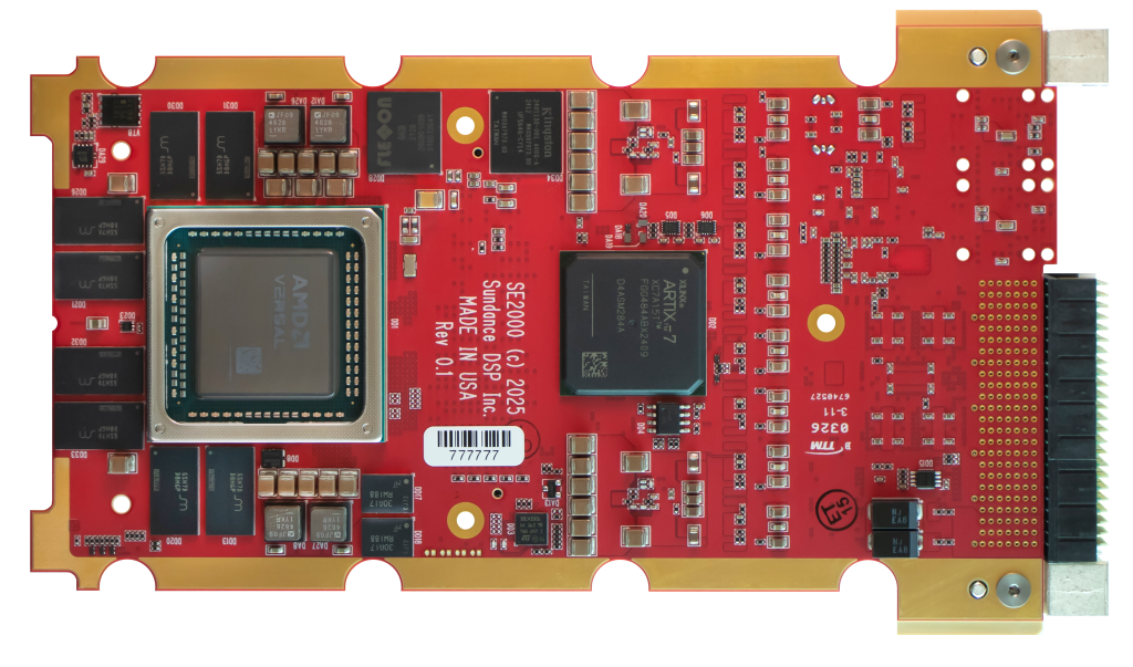
VNX+ (ANSI/VITA 90), formally ratified by ANSI and VITA in early 2026, exists precisely for that second case. It’s the direct successor to the original VNX standard (ANSI/VITA 74, ratified in 2017), which itself was built as a deliberately scaled-down derivative of VPX, same conceptual planes (utility, control, data, expansion, and I/O overlay), same philosophy of standardized module-to-backplane interconnect, but shrunk to modules roughly the footprint of a deck of playing cards.
VITA 74 proved the concept but hit real limits in the field: its practical thermal ceiling was pegged at around 20 W, which became a bottleneck as integrators started wanting to put genuinely capable 20–25 W processor modules into small platforms. The VITA 90 committee, working closely with the SOSA Consortium, used that field experience to define VNX+ as a more capable evolution rather than a patch. VNX+ modules are approximately 89 mm x 78 mm, available in single-height 12.5 mm and 19 mm stack heights (with double-height variants around 27 mm and 39 mm also defined in the standard for modules that need more component headroom), and are conduction-cooled by design, which removes the need for airflow across the board and makes them suitable for sealed, environmentally hardened enclosures. Thermal dissipation moved from VNX’s 20 W ceiling up to roughly 80 W in typical conduction-cooled configurations. Industry discussion of the standard also indicates headroom to as much as 95 W when advanced thermal mitigation, oscillating heat pipes, copper thermal paths, and similar techniques are applied. The connector and pin-mapping work of the VITA 74 technical committee, carried forward under the VITA 90 effort, optimized signal integrity for modern high-speed fabrics, PCIe Gen4, up to 100 Gbps Ethernet, and the kind of data-plane bandwidth that a serious edge-AI or sensor-processing payload now needs, though actual throughput on any given module or adapter still depends on the specific SOSA profile and connector configuration implemented.
Critically, VNX+ was built using the same OpenVPX-style plane architecture as VPX: utility plane, control plane, data plane, expansion plane, and I/O overlay, rather than inventing a parallel and incompatible signaling philosophy. VNX+ was also folded directly into the SOSA Technical Standard, first as VNX Plug-In Cards (PICs) in SOSA 1.0 and subsequently formalized under VITA 90. That shared lineage is precisely what makes the two standards electrically and architecturally compatible siblings rather than unrelated form factors that happen to both be rugged.
The target market for VNX+ is anything where VPX’s card size simply won’t physically fit: small UAVs and UUVs, gimbal and pod-mounted sensor payloads, man-wearable and dismounted soldier systems, artillery-launched or air-dropped sensor packages, cubesats and other small-satellite buses, and any C5ISR payload that has to squeeze into a tube, pod, or enclosure measured in centimeters rather than rack units. These are applications where VPX’s 3U footprint is simply too large, but where the program still wants the reliability, openness, and multi-vendor interoperability that VPX-derived architectures are known for.
The Size Relationship: Why VNX+ Fits Inside VPX’s Envelope
This is the mechanical fact that makes coexistence practical rather than theoretical. A VNX+ module’s footprint, roughly 89 mm x 78 mm, is physically smaller in both dimensions than even the smallest standard VPX card, the 3U OpenVPX outline at 100 mm x 160 mm. A VNX+ module can sit entirely within the front-panel and card-cage envelope that a 3U VPX slot already provides, with room to spare in the depth dimension.
That size relationship means a VNX+ module doesn’t need its own chassis, its own backplane standard, or its own power infrastructure to be usable in a VPX-based program. It needs a mechanical and electrical adapter that translates the VNX+ module’s 400-pin SBCIO connector interface into whatever the OpenVPX backplane slot expects, and holds the smaller module rigidly in the 3U card-cage envelope so it survives shock and vibration testing exactly like a native VPX card would.
SundanceDSP’s VNX+ to 3U VPX Adapter
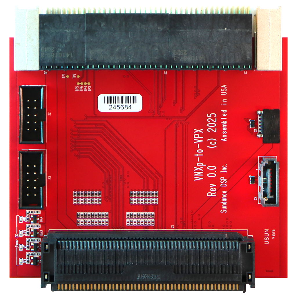
That’s exactly the role SundanceDSP’s VNX+ to 3U VPX Adapter plays. VNX+ itself supports several connector configurations across the standard, with different pin counts and row arrangements depending on module height and application; the SundanceDSP adapter specifically targets the 19 mm, 400-pin SBCIO Plug-In Module (PIM) variant. It’s built as a precision-engineered interposer and mechanical carrier between that 19 mm, 400-pin VNX+ PIM and a SOSA-aligned OpenVPX payload slot, specifically matching the SOSA payload profile MOD3-PAY-1F1F2U1TU1T1U1T-16.2.15-1. A VNX+ module plugs into the adapter, and the adapter itself plugs into a standard 3U OpenVPX backplane slot; no changes to the backplane, the chassis, or the rest of the system are required.
A few things about the adapter are worth calling out for anyone evaluating it:
- It’s fully passive. There are no active components, no power regulation, and no signal conditioning on the board. Its job is purely mechanical and electrical translation, connector alignment, form-factor conversion, and direct signal pass-through between the VNX+ PIM connector and the corresponding OpenVPX interfaces. That matters for reliability: a passive interposer introduces no new failure modes, no firmware, and no additional power budget to account for.
- Signal mapping is largely one-to-one. The OpenVPX control-plane (CPtp) lanes connect through to the VNX+ module’s Ethernet port lanes; the VNX+ S2 Overlay Mezzanine I/O pins (21 pairs total) route out to the XMC interface; the S2 video plane maps to the OpenVPX video plane; USB 3.0 and a second USB 2.0 port are routed through; and SATA port 1 is carried across as well. Power-rail LED indicators for 12 V, 5 V, and 3.3 V give a quick visual health check without needing test equipment.
- It’s rated for real deployment conditions. The adapter supports an operating range of 0°C to +70°C in its extended-temperature configuration and −40°C to +85°C in its industrial-grade configuration, which puts it squarely in the same environmental class as the VPX systems it’s designed to plug into.
- It preserves the mechanical envelope. Once assembled, the VNX+ module and adapter combination fits within the standard VPX chassis card-cage envelope, so it can be qualified, handled, and racked using the same mechanical procedures as any other 3U VPX card. That said, the combined assembly still has to satisfy the host chassis’s own mechanical retention (wedge locks, card guides) and conduction-cooling interface requirements; the adapter solves the electrical and form-factor translation, but the chassis-level thermal and mechanical qualification is still the integrator’s responsibility.
What Coexistence Looks Like in a Real System
In practice, this means a system architect isn’t choosing between VPX and VNX+ for a program; they’re choosing where each belongs. A 6U OpenVPX chassis built around a SOSA-aligned backplane can host native 3U and 6U VPX cards for heavy processing and switching workloads, FPGA-based signal-processing boards, single-board computers, and network switches, while reserving one or more payload slots for a VNX+ module carried on an adapter like SundanceDSP’s. That VNX+ slot might host a compact sensor-interface card, an RF front end, or a specialized processing module that was originally developed for a small-platform program and needs to be reused without a redesign.
This is particularly valuable for programs that span multiple platforms. A sensor processing module developed in VNX+ form factor for a UAV pod doesn’t need a second, VPX-native design to also be usable in a ground vehicle’s 3U VPX rack; the adapter lets the same qualified module serve both. That’s a meaningful cost and schedule advantage in defense and aerospace programs, where requalifying a board for a second form factor is expensive and slow, and where SOSA’s whole premise is reducing that kind of duplicated non-recurring engineering.
It also works in the other direction during development: engineers building or evaluating a VNX+ module can use standard 3U OpenVPX lab infrastructure, chassis, power supplies, and backplane test fixtures to bring the module up and debug it, rather than needing dedicated VNX+ bench hardware before a full small-form-factor enclosure is available. The adapter effectively turns a general-purpose VPX lab into a VNX+ development and test bench.
A Shared Governance Model: Why SOSA Ties Them Together
None of this coexistence would be practical if VPX and VNX+ were governed as separate, unrelated ecosystems. They aren’t. Both fall under the same VITA standards umbrella, and both are formally recognized building blocks of the Sensor Open Systems Architecture (SOSA) Technical Standard, which defines slot profiles, plug-in card (PIC) types, and interoperability rules across form factors rather than just within one. SOSA’s payload slot profiles, like the MOD3-PAY-1F1F2U1TU1T1U1T-16.2.15-1 profile the SundanceDSP adapter targets, exist specifically so that a VNX+ PIC can present itself to a 3U OpenVPX backplane in a predictable, standardized way, rather than requiring a one-off, program-specific translation layer.
That shared governance is also why the adapter concept scales beyond a single vendor’s product line. Because both VPX and VNX+ modules built to their respective ANSI/VITA and SOSA profiles expose known, published pinouts and plane assignments, an interposer board only has to solve the mechanical and electrical translation once; for a given pair of profiles, it doesn’t need to reverse-engineer a proprietary interface on either side. That’s a direct benefit of open, published standards over closed or vendor-specific small-form-factor designs, and it’s a large part of why defense and aerospace primes have converged on SOSA-aligned VPX and VNX+ hardware for new programs rather than continuing to design bespoke enclosures for every new platform.
Conclusion
VPX and VNX+ aren’t rival standards fighting for the same design win. VPX (VITA 46/65) is the mature, high-density backbone for systems where chassis space is available and multi-vendor interoperability at scale matters most. VNX+ (ANSI/VITA 90) is its small-form-factor sibling, built on the same architectural planes and aligned with the same SOSA Technical Standard, but shrunk and thermally re-engineered for platforms where every cubic centimeter counts. Because a VNX+ module’s footprint is smaller than even a 3U VPX card, it can physically live inside a VPX chassis with the right mechanical and electrical translation, which is exactly what a passive interposer like SundanceDSP’s VNX+ to 3U VPX Adapter provides. For system integrators, that means one architecture, two form factors, and no compromise on either side.