
If you’ve built a transmit-and-receive system around an FPGA carrier, you know the squeeze. There are only so many FMC sites and gigabit transceivers, and the DAC and ADC end up competing for both. SundanceDSP’s answer is to stack the ADC module on top of the DAC module so both share one FMC+ site on the PCIe104Z+ carrier.
The three boards
The carrier
The PCIe104Z+ is a PCIe/104 board, typically 90 × 96 mm, built around a Zynq UltraScale+ MPSoC. You can order it with a ZU7EV, ZU7EG, ZU11EG or ZU7CG. Its FMC+ (VITA 57.4) site brings out 18 GTH transceivers at up to 16.3 Gb/s and 80 LVDS pairs. A PCIe Gen3 x2 link goes to the programmable logic, with Gen4 available through custom IP. The processor side takes up to 8 GB of DDR4 and eMMC, and the logic side takes up to 4 GB of DDR4. The industrial variants rate the Zynq itself for -40 °C to 100 °C.
The DAC module
The FMCP-DAC12p0 has two AD9172 DACs, which gives four 16-bit channels. The board uses JESD204B and supports Subclass 1. It has an HMC7044 for clocking, a 100 MHz VCXO, a 10 MHz TCXO or external reference, and a trigger input. Sixteen ten-gigabit pairs run from the carrier to the DACs. On the solder side, a second carrier-type FMC+ connector accepts the ADC module.
The ADC module
The FMCP-ADC3p0 has two AD9208 ADCs, which give four 14-bit channels at 3 GS/s. It also uses JESD204B and an HMC7044. The AC-coupled differential inputs go straight to the converters without a balun, keeping the front end clean. Input impedance is 200 Ω differential, the default full-scale is 1.7 V differential, and the module’s maximum AC-coupled differential input is 2 Vpp. The module’s estimated maximum dissipation is 20 W.
The ADC comes in many variants: FMC+ or two-channel FMC, 2.0, 2.6, or 3.0 GS/s, single-ended or differential inputs, and extended or industrial temperature grades. The default part on the product is the FMCP-ADC2p0, a four-channel single-ended 2.0 GS/s module.
How they connect
PCIe104Z+ (Zynq UltraScale+)
   |  FMC+ mezzanine connector
   v
FMCP-DAC12p0  - 4 DAC outputs, clock/trigger, own HMC7044
   |  carrier-type FMC+ connector (solder side)
   v
FMCP-ADC3p0   - 4 ADC inputs, clock/trigger, own HMC7044
The photo of the combination includes an FMC+ interposer. The interposer adds SFP+ ports and a second FMC+ site.
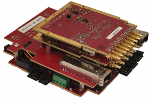
For lanes, the piggyback arrangement lets the carrier use both its transmit and receive transceivers.
What you get from the stack
One FMC+ site feeds both converters, so a full transmit-and-receive chain fits on a compact carrier without a second mezzanine site. The DAC board’s second connector gives the ADC access to the same site, which lets the carrier’s transmit and receive lanes serve both.
Both boards carry an HMC7044 and support JESD204B Subclass 1, which is the right starting point for tight timing.
Each module has a trigger input too. On the ADC, it can timestamp the sample stream, and on the DAC it can start the output on an event. The two inputs differ electrically:
| DAC trigger | ADC trigger | |
|---|---|---|
| Max input voltage | 3.3 V | 6 V |
| Logic “0” | < 0.4 V | < 0.8 V |
| Trigger threshold | > 1 V | > 2 V |
Both are DC-coupled, single-ended, 3.3 V logic, and work from DC to 10 MHz.
The ADC can also be ordered as a two-channel FMC part, and SundanceDSP lists an FMC+ to FMC adapter. The four-channel stack needs the FMC+ ADC.
Reference designs and integration work
The product comes with two separate Vivado projects, both built on the Xilinx JESD204B IP core. The DAC project sends sample signals out to the DACs. The ADC project captures samples and sends them to the host over PCIe.